PhD. Bhardwaj Jyoti, Senior Vice President, R&D, Philips Lumileds gives detailed information about the development of chip scale package technology in this article. Chip scale packages are novel to the LED industry but they are the mainstay of the semiconductor industry. Development of CSP in the Si ICs was driven by miniaturization, improved thermals, higher reliability, and simply the need to connect to an ever increasing pin-count on an ever shrinking die. Chip Scale packages also enabled a reduction in device parasitic and allowed for ease of integration into Level 2 packaging. It is therefore a natural evolution for such packaging innovation to proliferate into other industries including the LED product space and therefore not surprising that Chip-scale packaging has made inroads into the LED industry recently released by Philips Lumileds. Other LED manufacturers also claim to be working on such LED device packages.
 |
|
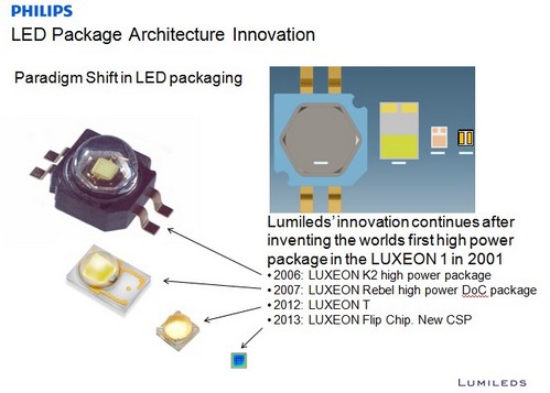
Development of Philips Lumileds LED packaging sizes from 2006 to 2013. (Photo Courtesy of Philips Lumileds) |
Chip scale packages are traditionally defined as fully functional packages that are of equal size or slightly larger than (<20%) the actual size of the die or in this case the active area of the LED. These packages typical do not require an additional sub-mount or substrate and can be directly attached to Level 2 boards. These Chip Scale packages are further characterized by having both P and N as bottom contacts and are surface mount devices (SMD) that can make use of standard packaging testing and s assembly equipment rather than wire bonds. Chip scale packages with their simplified standard spaced bonding pads enable standard testing and pick and place equipment to be used with similar cost and placement accuracy without adding complexity. This packaging gets even more attractive if the P and N pad spacing remains the similar to traditional QFN or lead frame packaging. CSP in its smallest form can be a Flip Chip device also referred to as Wafer Level packaging. The difference between the traditional Flip-Chip and a CSP flip chip is that the latter provides contact re-distribution within the die so that N and P contacts can be engineered for direct SAC or AuSn attach onto L2 without interposers or sub-mounts or any other form of additional packaging.
The dominant technology types for High Power LEDs have been based on thin film die (TFFC, EC-VTF and VTF) mounted on a ceramic package with a variety of phosphor technologies. The low and mid-power devices on the other hand have been driven primarily with a lateral die configuration with two wirebonds for contacts in lead frame or QFN packages employing dispense phosphor. A new LED architecture that is now being introduced for both Hi and Mid-power applications is the chip scale package (CSP) employing a flip chip configuration (CSP-FC).
|
|
|
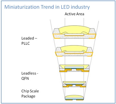
Package scaling. Traditional package migration path for semiconductor devices applied to LEDs shows that the CSP is the eventual end point. (Photo Courtesy of Philips Lumileds) |
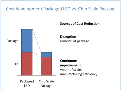
Similar to the semi-conductor industry, the LED industry strives for smaller and smaller devices but with the same light output and efficacy. Simply speaking, under these conditions, smaller is cheaper. In addition, depending on the applications, there are optical limitations on the size of the light emitting surfaces, especially in very high lumen devices such as chip-on-board applications. Chip-Scale packages provide the highest packing density and are SMD complaint for high speed low cost automatic attach.
The advantages of Chip scale package can be summarized as:
-
Better thermal contact to the substrate through Metal – metal interface of the bottom epi layer to the heat sink
-
Higher current densities, driving higher lumen output per device
-
High reliability with no wire bonds and a reduction in an attach process and package
-
Higher packaging density due to reduced footprint
-
Ease of integration on boards through surface mount technology
-
Flexibility of attach – AuSn, SAC, UBM
 |
|
Cost breakthrough with CSP. (Photo Courtesy of Philips Lumileds) |


 CN
TW
EN

