An emerging class of atomically thin materials known as monolayer semiconductors has generated a great deal of buzz in the world of materials science. Monolayers hold promise in the development of transparent LED displays, ultra-high efficiency solar cells, photo detectors and nanoscale transistors. Their downside? The films are notoriously riddled with defects, killing their performance.

|
|
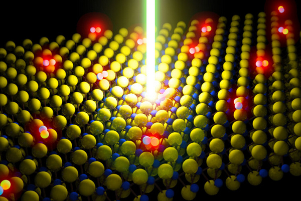
Schematic of a laser beam energizing a monolayer semiconductor made of molybdenum disulfide, or MoS2. The red glowing dots are particles excited by the laser. (Image courtesy of Der-Hsien Lien) |
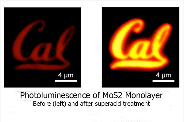
But now a research team, led by engineers at UC Berkeley and Lawrence Berkeley National Laboratory, has found a simple way to fix these defects through the use of an organic superacid. The chemical treatment led to a dramatic 100-fold increase in the material’s photoluminescence quantum yield, a ratio describing the amount of light generated by the material versus the amount of energy put in. The greater the emission of light, the higher the quantum yield and the better the material quality.
The researchers enhanced the quantum yield for molybdenum disulfide, or MoS2, from less than 1 percent up to 100 percent by dipping the material into a superacid called bistriflimide, or TFSI.
Their findings, to be published in the Nov. 27 issue of Science, opens the door to the practical application of monolayer materials, such as MoS2, in optoelectronic devices and high-performance transistors. MoS2 is a mere seven-tenths of a nanometer thick. For comparison, a strand of human DNA is 2.5 nanometers in diameter.
 |
|
Shown is a MoS2 monolayer semiconductor shaped into a Cal logo. The image on the left shows the material before it was treated with superacid. On the right is the monolayer after treatment. The researchers were able to achieve two orders of magnitude improvement in emitted light with the superacid treatment. (Image courtesy of Matin Amani) |
“Traditionally, the thinner the material, the more sensitive it is to defects,” said principal investigator Ali Javey, UC Berkeley professor of electrical engineering and computer sciences and a faculty scientist at Berkeley Lab. “This study presents the first demonstration of an optoelectronically perfect monolayer, which previously had been unheard of in a material this thin.”
The researchers looked to superacids because, by definition, they are solutions with a propensity to “give” protons, often in the form of hydrogen atoms, to other substances. This chemical reaction, called protonation, has the effect of filling in for the missing atoms at the site of defects as well as removing unwanted contaminants stuck on the surface, the researchers said.
Co-lead authors of the paper are UC Berkeley Ph.D. student Matin Amani, visiting Ph.D. student Der-Hsien Lien and postdoctoral fellow Daisuke Kiriya.
They noted that scientists have been pursuing monolayer semiconductors because of their low absorption of light and their ability to withstand twists, bends and other extreme forms of mechanical deformation, which can enable their use in transparent or flexible devices.
MoS2, specifically, is characterized by molecular layers held together by van der Waals forces, a type of atomic bonding between each layer that is atomically sharp. An added benefit of having a material that is so thin is that it is highly electrically tunable. For applications such as LED displays, this feature may allow devices to be made where a single pixel could emit a wide range of colors rather than just one by varying the amount of voltage applied.
 |
|
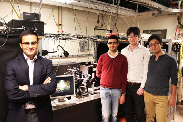
Ali Javey, UC Berkeley professor at the College of Engineering, and researchers in his lab have found a way to remove defects from atomically thin monolayer semiconductors. Shown, left to right, are Javey, Matin Amani, Der-Hsien Lien and Daisuke Kiriya. (Photo credit of Hiroki Ota) |
The lead authors added that the efficiency of an LED is directly related to the photoluminescence quantum yield so, in principle, one could develop high-performance LED displays that are transparent when powered off and flexible using the “perfect” optoelectronic monolayers produced in this study.
This treatment also has revolutionary potential for transistors. As devices in computer chips get smaller and thinner, defects play a bigger role in limiting their performance.
“The defect-free monolayers developed here could solve this problem in addition to allowing for new types of low-energy switches,” said Javey.
Xiang Zhang and Eli Yablonovitch, faculty members with joint appointments at UC Berkeley’s College of Engineering and Berkeley Lab, co-authored this paper. Other co-authors include researchers from National Taiwan University, the University of Texas and the U.S. Army Research Laboratory in Maryland.
The work was funded by the U.S. Department of Energy, the National Science Foundation Center for Energy Efficient Electronics and Science at UC Berkeley, Samsung and the Center for Low Energy System Technology.


