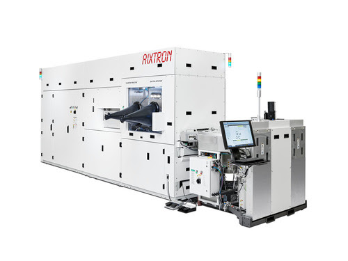
AIXTRON’s planetary technology sets the ground for the next generation of high-resolution Micro LED displays and lasers
AIXTRON SE (FSE: AIXA, ISIN DE000A0WMPJ6) launches the first fully automated AsP platform to the market. The new system G10-AsP addresses the growing demands in the fields of Micro LED and laser devices. As first system in the industry, the G10-AsP enables a robust high-volume production which is linked to very high and complex requirements.
“Micro LEDs will revolutionize the world of displays as they offer better durability, higher lifetime, a better picture quality and a very low energy consumption. However, this innovative technology challenges the production process as it requires lowest defect levels and highest uniformity rates. The answer to all this our new G10-AsP as it offers the industry’s first fully automated process. The new system enables the highest throughput of its class with uniformity and defect levels never seen before”, says Dr. Felix Grawert, CEO and President of AIXTRON SE.
For the first time, a true mass production of Micro LEDs with the most tightened material requirements and reduced chip sizes of 10 micron and lower is becoming a reality. Additionally, the G10-AsP also meets the complex requirements to produce InP (Indium phosphide) laser and VCSEL (Vertical Cavity Surface Emitting laser) in high volumes.
The new platform G10-AsP will officially be launched on 1st of February 2023 during the Photonic West exhibition in San Francisco, USA. During this event, AIXTRON experts will present the new system: They will explain all the innovations that are packed into the new platform and how it will provide the highest throughput of its class and maximize cleanroom utilization.
The new fully automated G10-AsP is the largest 200mm AsP Batch reactor released to the market and comes with In-Situ Cleaning and an automated cassette-to-cassette (C2C) wafer loading. For the first time, the Front-End can be equipped with SMIF (Standard Mechanical Interface) pods to further minimize the exposure of the epitaxial wafers to the room environment. With the In-Situ cleaning built-in, users can reset the chamber conditions on demand – be it after each process run for the most demanding requirements or just after a production campaign to benefit from highest throughputs. The platform is based on the successful Planetary Reactor® technology which combines the multiwafer batch reactor concept with single wafer rotation to guarantee highest wafer uniformity.
Micro LEDs will not only be used for the next generation of TV displays but also for future smart watches, smart phones, Augmented Reality (AR) projection or automotive displays. Analysts expect this area to be the largest market for LEDs in the next five to ten years.
The one big challenge to reach the next level for advanced Micro LEDs, but also for InP and VCSEL applications remains uniformity: Optimized on-wafer uniformity and wafer-to-wafer uniformity must be accomplished in a high-volume production process. The new G10-AsP sets a new standard with respect to these values, offering a two-to-threefold improvement compared to its predecessor. Hence, this fully automated platform will initiate a new era to produce Micro LED and photonic devices, overcoming major obstacles that previously have prevented a robust mass production.
Photonic devices such as infrared lasers and detectors have already been adopted broadly in the market. In telecommunications, they lay the foundation to manage ever-growing data volumes which are linked to continuously higher bandwidth requirements. Also, they enable 3D sensing, e.g., for facial recognition, and advanced technologies for autonomous driving: With the continuous evolvement of this technology, beams must map larger and wider areas. This calls for tighter wavelength tolerances which translate into very tight requirements for the epitaxial layer deposition. The new G10-AsP can address this need by providing a significantly refined control of the epitaxial process with improved material accuracy, reduced defects and as a result higher yield and better uniformity.
In the production of Micro LEDs, an improved uniformity is the prerequisite for economical viable mass production: Micro LED displays rely on a special stamp or matrix transfer process where thousands of LED chips (arrays) of just a few micrometers in size are picked up and transferred. Because entire arrays of pixels are transferred from the epi-wafer substrate, almost perfect uniformity is required – or could you imagine anyone purchasing a smartwatch or smartphone with a display having a different color in one corner than the other?

The new fully automated AIX G10-AsP is the largest 200mm AsP Batch reactor released to the market and comes with In-Situ Cleaning and an automated cassette-to-cassette (C2C) wafer loading.
Release date: 31 May 2022 / 30 November 2022
Format: PDF
Languages: Tradional Chinese / English
Pages : 130–150 in total (subject to change)
If you would like to know more details , please contact:


