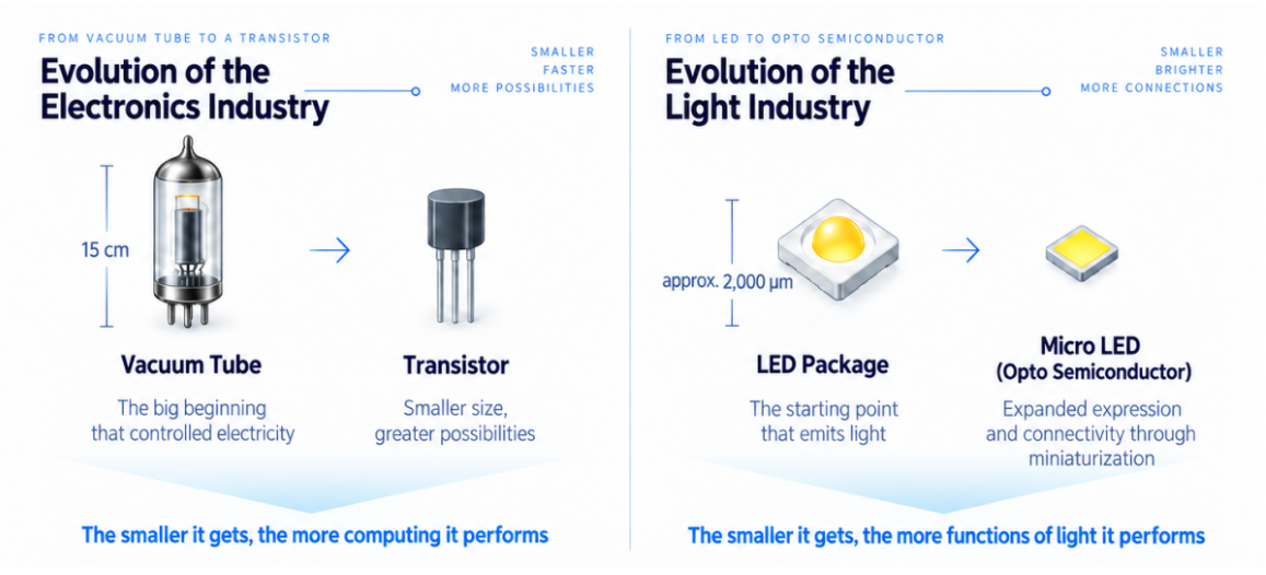
Just as the transition from a 15 cm vacuum tube to a 1 cm transistor triggered the IT revolution, light-emitting devices are also evolving beyond conventional LEDs used simply for illumination into ultra-miniaturized opto semiconductors that will drive the AI era.
Based on proprietary technologies developed in Korea, including WICOP, device dimensions have been reduced from conventional packages of approximately 2,000 µm to an extreme scale of 1 µm — roughly 1/2,000 of the original size.
These nearly invisible 1 µm opto semiconductors are expected to become key devices for high-speed AI communications, AR, and highly transparent displays, creating a market projected to reach $50 billion within the next decade — roughly one-quarter the size of the memory semiconductor market.
1. We Do Not Call a Transistor a Vacuum Tube: A Fundamental Paradigm Shift
When the bulky 15 cm vacuum tube was replaced by the fingernail-sized transistor, the world did not call it a “smaller vacuum tube.”
Today, the same transformation is taking place in the field of photonics.
The traditional concept of the LED — a light-emitting diode used simply to illuminate spaces or provide backlighting behind displays — is reaching its limits.
Light-emitting devices are now evolving into advanced opto semiconductors capable of transmitting data at ultra-high speeds and powering next-generation AI devices.
2. Korea’s Extreme Semiconductor Innovation: From 2,000 µm to the 1 µm Era
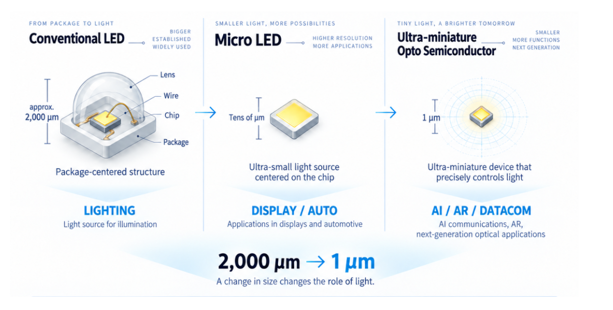
Conventional LEDs were built around relatively bulky structures in which a chip was mounted inside a thick plastic package and connected using gold wires.
Their overall size could reach approximately 2,000 µm because they were designed primarily as packaged components for producing visible light.
Korea-led proprietary technologies, including WICOP-based no-wire, no-package technology, eliminate unnecessary wires and packages and enable device dimensions to be reduced to an extreme 1 µm scale — about 1/2,000 of conventional packaged LEDs.
-
Conventional packaged LED (2,000 µm): A component mainly used for visible lighting and backlighting
-
Next-generation opto semiconductor (1 µm): Approximately 1/100 the thickness of a human hair, invisible to the naked eye, yet capable of supporting highly precise optical functions including ultra-high-speed data transmission
The device becomes almost invisible to the human eye, while performance, precision, and reliability continue to advance.
3. Three Future Innovations Enabled by 1 µm Opto Semiconductors
Extreme integration at the 1 µm scale enables applications that conventional LEDs could not achieve.
-
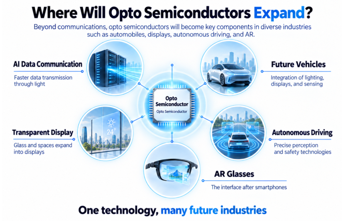
Ultra-lightweight, ultra-high-resolution AR glasses that could replace smartphones
To realize everyday AR devices in an eyewear form factor, millions of ultra-fine pixels must be integrated within an ultra-compact form factor and projected directly before the user’s eyes. 1 µm-scale opto semiconductors can dramatically increase pixel density while enabling high brightness even in daylight and reducing power consumption.
This could accelerate the transition from smartphones to the era of spatial computing.
-
Optical interconnects replacing copper bottlenecks in AI data centers
As generative AI models continue to grow, copper-based electrical connections are increasingly constrained by bandwidth, heat, and power consumption.
Optical interconnect technologies based on ultra-miniaturized opto semiconductors can connect chip-to-chip and board-to-board systems using light, offering significantly higher bandwidth and lower power consumption than conventional electrical transmission.
-
90% transparent displays that merge digital information with physical space
At dimensions as small as 1 µm, individual devices occupy only a minimal portion of the overall display area.
This can enable transparent displays with transmittance exceeding 90%, potentially transforming automotive windshields, smart-building glass, and augmented-reality windows into interactive displays.
4. A $50 Billion Market Within 10 Years — One-Quarter the Size of the Memory Semiconductor Market
This technological paradigm shift signals the emergence of a major new market.
-
Silicon (Si) semiconductors: $630B in 2025 → $1.21T in 2034
Memory: $200B / Non-memory: $1.0T
-
Compound semiconductors: $60B in 2025 → $150B in 2034
Among next-generation compound semiconductor technologies, the opto semiconductor market is expected to reach $50 billion, or approximately KRW 67 trillion, by 2034.
“It Is No Longer Just LED. It Is the Opto Semiconductor Opening the Future.”
(Photo credit: Seoul Semiconductor)
TrendForce 2026 Micro LED Display and Non-Display Application Market Analysis
Release: 15 September 2026
Format: PDF
Language: Traditional Chinese / English
|
If you would like to know more details , please contact:
|


