Scientists at the MPI-P Mainz, BASF Ludwigshafen, the University of Ulm, and Innovation Lab Heidelberg have developed a simulation toolkit for evaluating properties of organic light emitting diodes (OLEDs) based solely on their chemical composition. The package is integrated in the free software VOTCA and helps to pre-select suitable organic molecules for lighting and display applications.
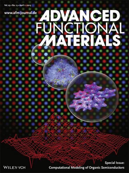
Mainz. The research group headed by Dr. Denis Andrienko, project leader at the Max Planck Institute for Polymer Research (Theory department, director Prof. Kurt Kremer) has developed a set of multiscale simulation techniques which predict macroscopic properties of an organic light emitting diode (OLED) from its chemical composition. The link between the molecular and mesoscopic scales became possible by combining advanced coarse-graining techniques with efficient simulation algorithms (see Figure). Implemented, among others, by the PhD candidate Pascal Kordt and postdoctoral fellow Dr. Jeroen van der Holst, this development facilitated computer simulations of electron and exciton motion in about 100 nanometer-thick OLED layers, i.e. macroscopically large, yet microscopically-resolved systems. The developed methods are reviewed in the feature article “Modeling of Organic Light Emitting Diodes: From Molecular to Device Properties” of Advanced Functional Materials, and highlighted as a cover page.
 |
|
Multiscale simulation of OLEDs. Small sphere and background: pixel structure of a Samsung Galaxy S5 mobile phone display. Middle sphere: atomistic morphology of an amorphous OLED layer. Wavefunction of a single-molecule. Bottom: energetic landscape for electrons. (All photos courtesy of AFM) |
Denis Andrienko explains how useful the software is to the organic semiconductors industry: “Modern mobile phones already use OLED (AMOLED), and large OLED-based TV screens are entering the market. Yet, the materials design for these applications often progresses via the trial-and-error strategy”, he explains. “In our approach both atomistic morphologies of amorphous OLED layers and charge motion are predicted solely from molecular structures. In contrast to experiments, OLED properties are then directly linked to the underlying chemistry and material morphology.” The expectation, backed up by the European Research Council and financially supported by the German Ministry for Education and Research (grant MESOMERIE, FKZ 13N10723), is that the computer-based design will rapidly grow in the coming years, allowing companies to save money on synthesis and characterization of new materials.
Interestingly, the 2014 Nobel Prize in Physics was awarded to Isamu Akasaki, Hiroshi Amano and Shuji Nakamura for the invention of efficient blue light-emitting diodes, or LEDs. LEDs are by now used as signal lights in alarm clocks, entertainment devices, flashlights, and more recently in large-area displays, where tiny red, green, and blue LEDs form a pixel. Millions of pixels are employed to display an image. In every pixel electrons constantly recombine with their counterparts (holes) and form photons, the elementary particle of light. Depending on the material, these photons have different energy, or wavelength, which then determines the light color. LEDs are made of inorganic materials and are therefore exceptionally stable. Recent developments in organic semiconductors illustrated that organic semiconductors can provide complementary material properties, e.g. high contrast ratios, curved shapes, or mechanical flexibility (bendable and foldable displays).
 |
|
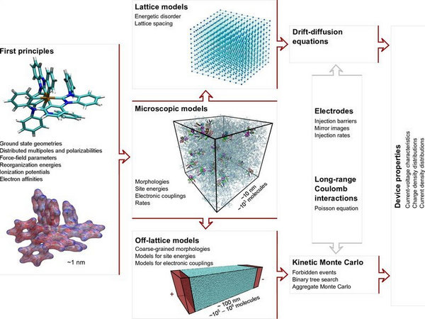
Possible workflows of parameter-free OLED simulations: polarizable force-fields and electronic properties of isolated molecules obtained from first principles are used to generate amorphous morphologies and evaluate charge transfer rates in small systems (microscopic models). Coarse-grained models are parametrized either by matching macroscopic observables, e.g., charge mobility, of the microscopic and coarse-grained (lattice) models. The resulting analytical expressions for mobility are then used to solve drift-diffusion equations for the entire device, after incorporating long-range electrostatic effects and electrodes. Alternatively, off-lattice models can be developed by matching distributions and correlations of site energies, electronic couplings, and positions of molecules. The master equations for this model can be solved using the kinetic Monte Carlo algorithm, yielding macroscopic characteristics of a device. |
The task of computer simulations is to help designing new materials for OLEDs. Even with modern supercomputers, however, it is impossible to simulate an OLED with the full atomistic detail. To remedy the situation, multiscale schemes are employed: properties of a single molecule are evaluated using first principle methods. Subsequently, a classical molecular model is parameterized and used to study systems of thousands molecules. OLED layers, however, consist of 100 nanometer thick layers (millions of molecules). In VOTCA, an intermediate stochastic model is introduced, which reproduces distributions of important microscopic properties (e.g. distances between molecules), and is then employed to simulate an entire OLED device.
In spite of the clear roadmap in designing new materials for OLEDs, the methods and code development are always “under construction”, which makes it an interesting and exciting research topic.


