JBD, a Hong Kong based technology startup company, reports the realization of monochromatic red, green and blue active matrix micro-LED (AMµLED) micro-displays with >5,000 dpi pixel density using wafer scale monolithic hybrid integration process.
Challenges
The emerging applications of wearable electronics and augmented reality (AR) raise an urgent call for new display technologies. The miniaturized displays that can be accommodated to those market applications need to meet stringent technical requirements that cannot be satisfied by current technologies. Micro-LED micro-displays which are gaining considerable traction in recent years are viewed as one of promising solutions. As a self-emissive display technology, micro-LED micro-displays are more compact in size, fast in response time and can provide higher contrast ratio and energy efficiency compared with LCD and LCoS technologies. Meanwhile, compared to OLED micro-displays which are also selfemissive, micro-LED micro-displays excel in higher brightness and reliability.
Currently, to produce those micro-LED micro-displays, hybridization of micro-LED arrays with CMOS active matrix (AM) driver ICs using flip-chip technology is one of major solutions. However, there are several main drawbacks in this manufacturing method. First, flip-chip is a chip-level process, making it a low through-put hence high cost process. Second, the thermal mismatch between the LED epi substrate and Si substrate of ICs introduces build-in stress during the bonding process, which may cause manufacturing yield loss and long-term reliability issues to the hybrid chips. Furthermore, limited by the alignment accuracy of the bonding equipment, it is difficult to push the pixel pitch down to a few microns. For applications in AR that requires ultra-compact high resolution micro-displays with pixel pitch of 5µm or below, a new manufacturing approach is needed.
JBD’s Solution
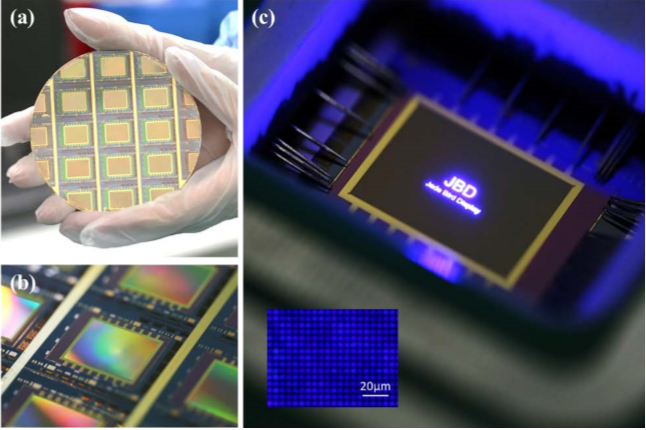
To address those challenges, JBD has developed its monolithic hybrid integration technology. Through wafer bonding followed by substrate removal processes, JBD has successfully transferred the functional compound semiconductor epi layers onto Si IC wafers. Such wafer-level blank epi transfer eliminates the need of precise alignment as required by flip-chip technology, therefore makes it high throughput waferlevel process suitable for large volume and low-cost production. The resulted epi-on-IC templates are subsequently subjected to the standard semiconductor fabrication processes with high alignment accuracy to produce monolithic hybrid optoelectronics integrated circuit (OEIC) chips.
 |
|
Figure 1. (a) A 4-inch wafer with 9 AMµLED micro-display chip dies; (b) Photo of a close look of the AMµLED micro-display chip on the wafer; (c) Photo of a blue AMµLED micro-display chip displaying image during a waferlevel die test. (Image: JBD) |
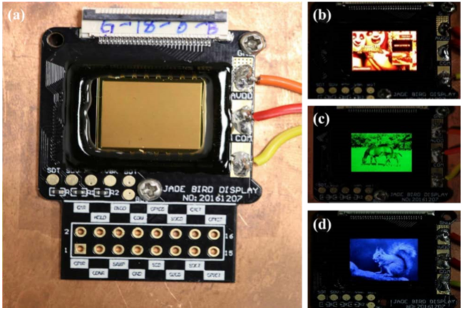
Using JBD’s monolithic hybrid integration technology, monochromatic red, green and blue micro-LED micro-displays have been successfully demonstrated on Si based AM micro-display IC backplanes. The AMµLED micro-displays have achieved high resolution with 5µm pixel pitch. The brightness of the AMµLED micro-display (green) demonstrated well exceeds 500,000cd/m², representing an improvement of over 500-times compared to the existing self-emissive micro-displays. And with further optimization of the device design and fabrication process, JBD’s solution can lead to micro-LED micro-displays with even higher resolution of over 10,000 dpi, which will make the most desirable and promising solution for various wearable electronics and AR applications.
 |
|
Figure 2. (a) Photo of AMµLED micro-display after wire bond and packaging on the control circuit board; Photos of AMµLED micro-displays displaying images: (b) Red micro-display; (c) Green micro-display; (d) Blue microdisplay (Image: JBD) |


