Ian Williams, Linear Applications Engineer at Texas Instruments tackles printed circuit board (PCB) solder flux issues that affect circuit functionality in a recent blog entry. When troubleshooting non-functional or poorly performing circuits, engineers often run simulations or other analyses that consider the circuit at the schematic level. If these methods fail to resolve the issue, even the best engineer might be left feeling stumped, frustrated, or confused. I’ve felt this pain myself. To prevent you from reaching a similar dead end, I present to you one simple, but crucial, tip: keep it clean!
What do I mean by this? Well, some materials used during the printed circuit board (PCB) assembly or modification process can cause major issues in circuit functionality if the PCB is not properly cleaned. One of the most common culprits of this phenomenon is solder flux!
 |
|
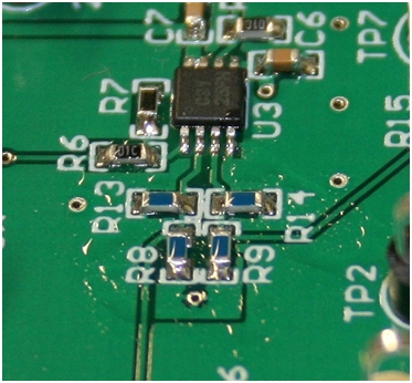
Figure 1 shows a PCB with an excess amount of residual solder flux. (LEDinside/Texas Instruments) |
Solder flux is a chemical agent used to facilitate the soldering of components to a PCB. Unfortunately, if not removed after soldering, flux can also deteriorate the surface insulation resistance of the PCB – wreaking havoc on the performance of your circuit in the process!
 |
|
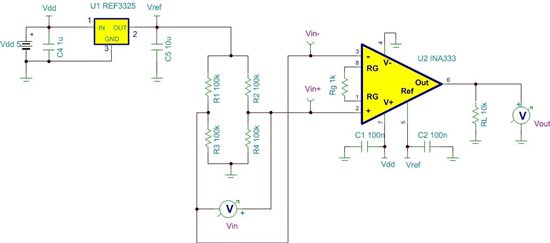
Figure 2 shows the test circuit Williams used to illustrate the effects of solder flux contamination. |
Figure 2 shows the test circuit I used to illustrate the effects of solder flux contamination. A balanced Wheatstone bridge network, excited by a 2.5 V reference, simulates a high-impedance bridge sensor. The differential bridge sensor output, VIN+ - VIN-, is connected to the INA333 with gain = 101 V/V. Ideally, VIN+ - VIN- = 0V since the bridge is balanced. However, flux contamination causes the actual bridge sensor voltage to slowly drift over time.
In this test, I simultaneously recorded VIN- and VOUT over one hour after various levels of cleaning after assembly:
-
No cleaning
-
Hand cleaning and air dry
-
Ultrasonic bath, air dry, and bake
 |
|
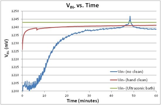
Figure 3 impact of solder flux contamination on bridge sensor output. (LEDinside/ Texas Instruments) |
As you can see in Figure 3, the solder flux contamination had a drastic impact on the behavior of the bridge sensor output! With no cleaning and hand cleaning, the bridge sensor voltage never reached its expected voltage of roughly VREF/2, even after an hour of settling time. The non-cleaned board also exhibited a large amount of external noise pickup. After cleaning it in the ultrasonic bath and allowing it to fully dry, the bridge sensor voltage was rock-solid.
 |
|
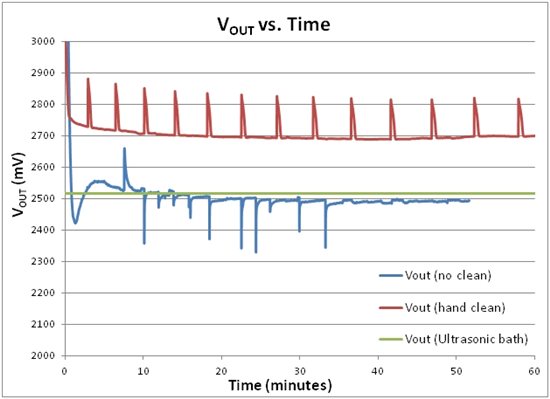
Figure 4 of the PCB solder flux test. (LEDinside/ Texas Instruments) |
Observing the output voltage of the INA333, we continue to see performance degradation with improper cleaning.
-
The board with no cleaning showed dc errors, very long settling time and significant external noise pickup.
-
The hand-cleaned board showed strange very-low-frequency noise. I eventually determined the cause – the air-conditioning cycling inside the test facility!
-
As expected, the properly cleaned and baked board performed perfectly and did not shift at any point during the test.
In summary, improper cleaning of solder flux can cause major performance degradation, especially in precision dc circuits. Remember to use an ultrasonic bath (or similar) for final cleaning of all hand-assembled or reworked PCBs. After drying with an air compressor, bake assembled and cleaned PCBs at slightly elevated temperature to remove any residual moisture. We typically bake for 10 minutes at 70°C.
This one simple tip of “keep it clean” should help you spend significantly less time troubleshooting and more time designing awesome precision circuits!


