Rubicon announced the launch of the first commercial line of large diameter patterned sapphire substrates (PSS) in four-inch through eight-inch diameters. This new product line provides LED chip manufacturers with a ready-made source of large diameter PSS to serve the needs of the rapidly growing LED general lighting industry.
 |
 |
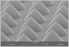
small patterned sapphire substrate
|
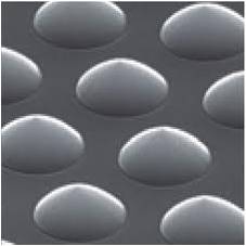
big patterned sapphire substrate
|
“As LED-based general lighting gains worldwide adoption, large-diameter patterned sapphire substrates will become necessary to meet the demands of the rapidly growing lighting market”
Growth of the LED general lighting market is expected to expand from nearly 300 million lamps shipped in 2012 to 3 billion by 2020 according to IMS Research. Technology innovation is helping the LED supply chain prepare for this dramatic growth. Most high-brightness LED manufacturers etch a pattern into the sapphire wafers in order to both improve epitaxial growth and extract more light from each chip. Patterned sapphire substrates have been available for purchase in smaller diameters, but Rubicon is the first to offer highly customizable 6” and 8” PSS. The larger substrates increase chipmakers’ throughput and efficiency.
“As LED-based general lighting gains worldwide adoption, large-diameter patterned sapphire substrates will become necessary to meet the demands of the rapidly growing lighting market,” said Raja M. Parvez, president and CEO of Rubicon Technology. “Rubicon has developed an unmatched technology platform that is vertically integrated from raw material through crystal growth, large diameter polished wafers, and now custom PSS in 4”, 6” and 8” diameters. Our vertical integration enables Rubicon to produce progressively larger sapphire products while providing customers with exceptional quality, cost control, reliability, and consistency.”
Rubicon offers fully customizable sub-micron patterning capability with tight dimensional tolerances, within ±0.1 µm. With an edge exclusion zone as small as 1 mm, Rubicon offers LED chip manufacturers more usable area to maximize the number of chips per wafer.


