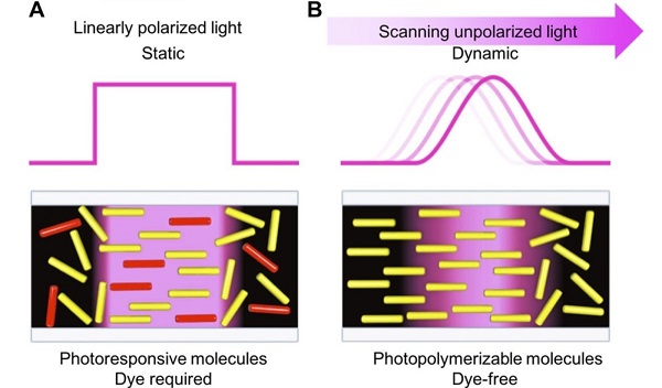
Scientists at Tokyo Institute of Technology (Tokyo Tech) and McGill University have developed a new dye-free photoalignment method that enables 2D patterns of liquid crystals in one step by guiding nonpolarized light temporally and spatially on the photopolymerization process. This new method provides a pathway for the simple creation of highly functional organic materials such as flexible liquid crystal devices.
With current 2D techniques, one typically irradiates a liquid crystal film that contains added photoresponsive dye molecules, with uniform polarized light. This controls the net liquid crystal alignment via the interaction of the dye dipole and the polarization axis of light. The drawback with these systems is the need for adding strong dyes, which can discolor or degrade optical and stability properties. Thus, a dye-free method is highly desired in the engineering industry.
 |
|
Schematic representations of photoirradiation for controlling molecular alignment. A represents the molecular alignment through conventional photoalignment methods. B represents the molecular alignment achieved through the currently reported scanning wave photopolymerization method. (Image: Tokyo Institute of Technology) |
Currently, only two approaches to dye-free methods have been explored. The first is a two-step alignment method, in which the liquid crystal materials are coated over a very thin dye-containing photoalignment layer and then aligned or fixed by polymerization. While this method has proven very successful in achieving stimuli-responsive 2D aligned liquid crystals and elastomers used in photonics, solar energy harvesting, microfluidics, and soft-robotic devices, it is expensive and time-consuming. The creation of a film with microscopic arrays of microalignment patterns requires precise and dynamic control of the polarized direction of incident light in each pixel, so this method is unsuitable for aligning patterns on the nanoscale over large areas.
The second approach to the development of a dye-free system uses surface topography to overcome the limitations of conventional photoalignment. In this method, the liquid crystals are aligned over a surface topography template through lithography, nanoimprinting, or inkjet techniques among others. While this method allows for 2D micropatterning of molecular alignment, it still requires multi-step processing, making it costly and time-consuming. Due to the surface roughness from the topographic templates, this method proves difficult in the production of thin films.
A research group led by Atsushi Shishido at Tokyo Tech has reported the development of a new method of scanning wave photopolymerization that utilizes spatial and temporal scanning of focused guided light. As the polymerization reaction proceeds, a mass flow in the film is triggered, and this results in alignment of the liquid crystals with the incident light patterns. The desired alignment is achieved through a single step by light triggered mass flow.
This new method generates arbitrary alignment patterns with fine control over larger areas in a wide variety of liquid crystal materials without the need for strong dyes or additional processing steps, something that previous methods were unable to achieve. This method has the additional advantage of unlimited complexity in 2D patterns that would, in principal, only be restricted by the light diffraction limits.
This new concept of scanning wave photopolymerization is currently limited to photopolymerizable liquid crystal systems with a thickness below tens of micrometers. However, further investigation can expand material systems that could be used such as nanorods, nanocarbons, and proteins. Scanning wave photopolymerization can be readily introduced into existing photoproduction facilities, allowing for great economic advantages. The scientists at Tokyo Institute of Technology see this method as a powerful pathway for the simple creation of highly functional organic materials with arbitrary, fine molecular alignment patterns on the nanoscale over large areas.


