In the manufacturing process of Micro LED display, inspection and repair technologies are indispensable to enhance and assure production yield. But again, given the massive amount of Micro LED chips in tiny size, Micro LED display makers face a great challenge for the testing and repairing process.
LED testing includes photoluminescence (PL) and electroluminescence (EL) tests. The former method can test LED chips without touching and ruining them but it might not detect all the defects compared to EL test. On the contrary, EL tests are able to identify more defects but they test LED chips by setting up electric currents which requires touching the LED chips that might lead to chip damages. For Micro LED inspection, applying EL tests are very difficult and slow as the chip size is too small for conventional testing equipment. But using PL tests might miss some defects, resulting in lower efficiency.
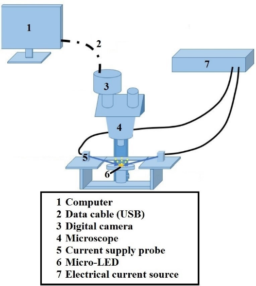
Therefore, technology developers and equipment makers are working on mass testing techniques to improve inspection efficiency without damaging the chips. A joint research team of Xiamen University in China and National Chiao Tung University has developed a camera-based microscopic imaging system for Micro LED testing. Integrating a computer, electrical current source, digital camera, current supply probe, and microscope with supporting software, the system can capture and analyze the photomicrograph to measure the luminance of Micro LED chips.
The Konica Minolta Group who specialized in equipment manufacture has also begun Micro LED and Mini LED inspection system development with its subsidiaries Instrument Systems (Germany) and Radiant Vision Systems (US). The group covers a wide range of inspection applications including gamma tuning, uniformity and LED chip inspection.
Since Micro LED chip dies are small, how to efficiently repair and replace bad dies after identifying them is also a challenging task. Currently, Micro LED repairing solutions include ultraviolet irradiation repairing technology, laser welding repairing technology, selective pick repairing technology, selective laser repairing technology and redundancy circuit design solution are used by Micro LED display makers to solve the defect issue.
US startup Tesoro proposed its approach of in-process testing which combine non-contact EL testing and Beam-Address Release (BAR) transfer method which is able to transfer only good Micro LED chips onto targeted substrate in high speed.
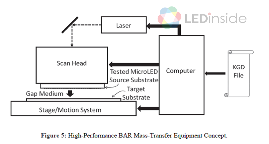
(Image: Tesoro)
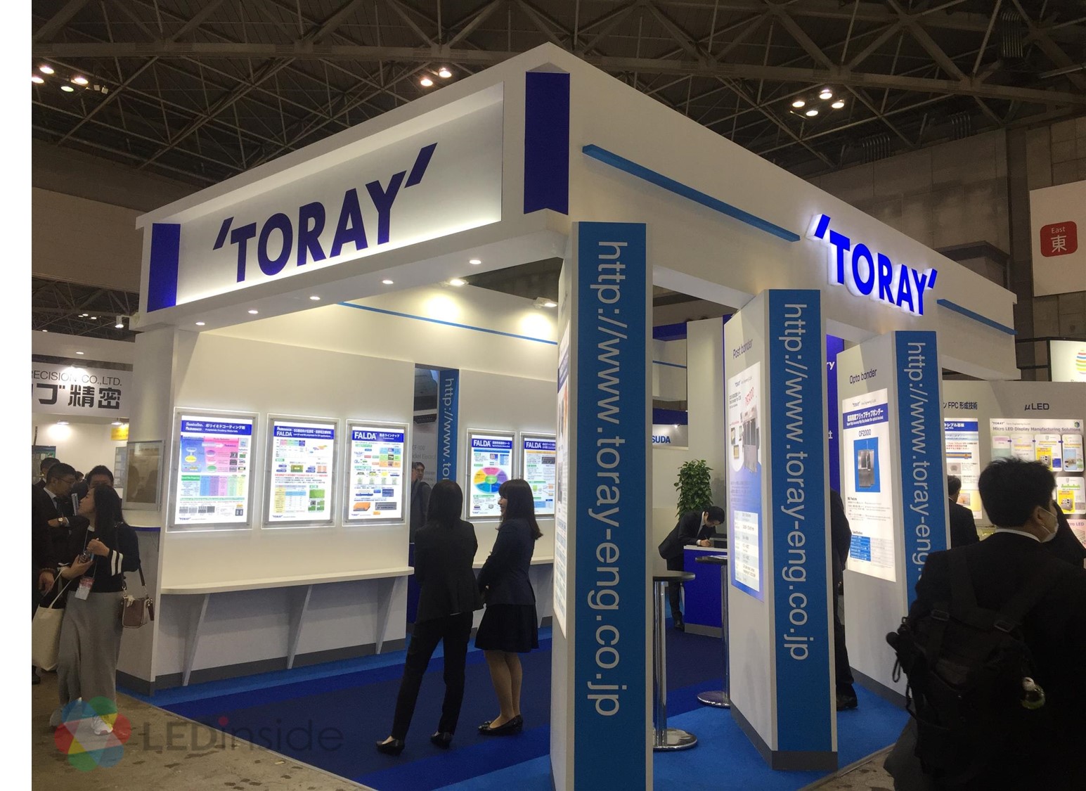
Japanese equipment maker Toray introduced its solutions for Micro LED inspection and repairing. Its auto optical inspection tool enables non-contact inspection, and then its laser trimming tool could exclude failed Micro LED chips according to inspection result.
Roger Chu, Research Director of LEDinside, indicated that most of the production cost of Micro LED display comes from repairing and mass transferring. He further noted that to reach the goal of higher yield, overall improvement in the production process, from epitaxy wafer to mass transferring, is still the key.
Toray and Konica Minolta will present their technology advancements and solutions for overcoming Micro LED display difficulties at Micro LEDforum 2019 held by LEDinside. Discover more updated Micro LED technology solutions with us; register now for early bird offer!