In the first half of 2020, the COVID-19 pandemic has heavily impacted the world as well as the technology industry with various interruptions occurred in the supply chain. In April, LEDinside covered how Micro LED technology could still have a chance to grow despite the COVID-19 impacts on the industry. And now, we would like to share the breakthroughs of Micro LED unveiled during the first half of the year proving that developments of the technology have not stopped by the pandemic.
Micro LED Wafer and Chip Improvements
Researchers have been working on improve Micro LED wafer or chip production to tackle the fundamental issues of efficiency, full color delivering as well as other challenges with the aim to reduce difficulties in following production process.
InGaN Micro LED is a field where many worldwide researchers are dedicating to. Earlier this year, researchers at University of Sheffield in the UK reported a new production method to develop Micro LED epiwafer that enables multi-color Micro LED arrays on single wafers with high light efficiency and uniformity. The technology will be deployed by the spin-out company of the university, EpiPix, to driver commercial applications.
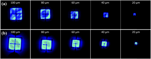
Lately, UCSB also announced a new research on high efficiency InGaN blue Micro LED development. The researchers advanced MOCVD growing process and used selective area growth (SAG) to fabricate InGaN Micro LED with epitaxial tunnel junctions which achieved better performance.

(Li et al. 2020)
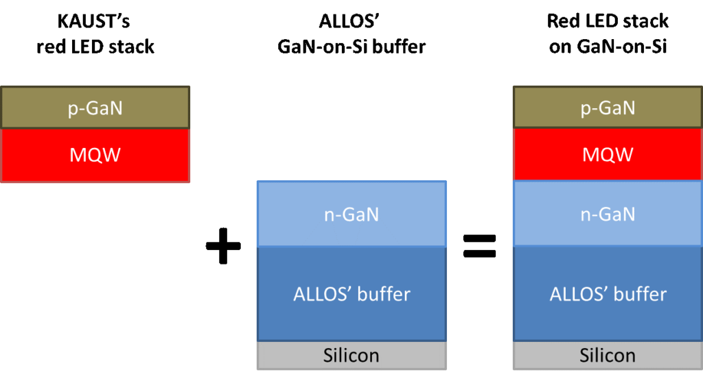
Moreover, KAUST continues its development of red InGaN Micro LED and announced several breakthroughs in the first half of 2020. The team achieved a peak wavelength of 665 nm with its InGaN red Micro LED and presented a stabilized structure afterwards. The researchers are now collaborating with ALLOS to develop InGaN red Micro LED on silicon substrate.

(Image: ALLOS)
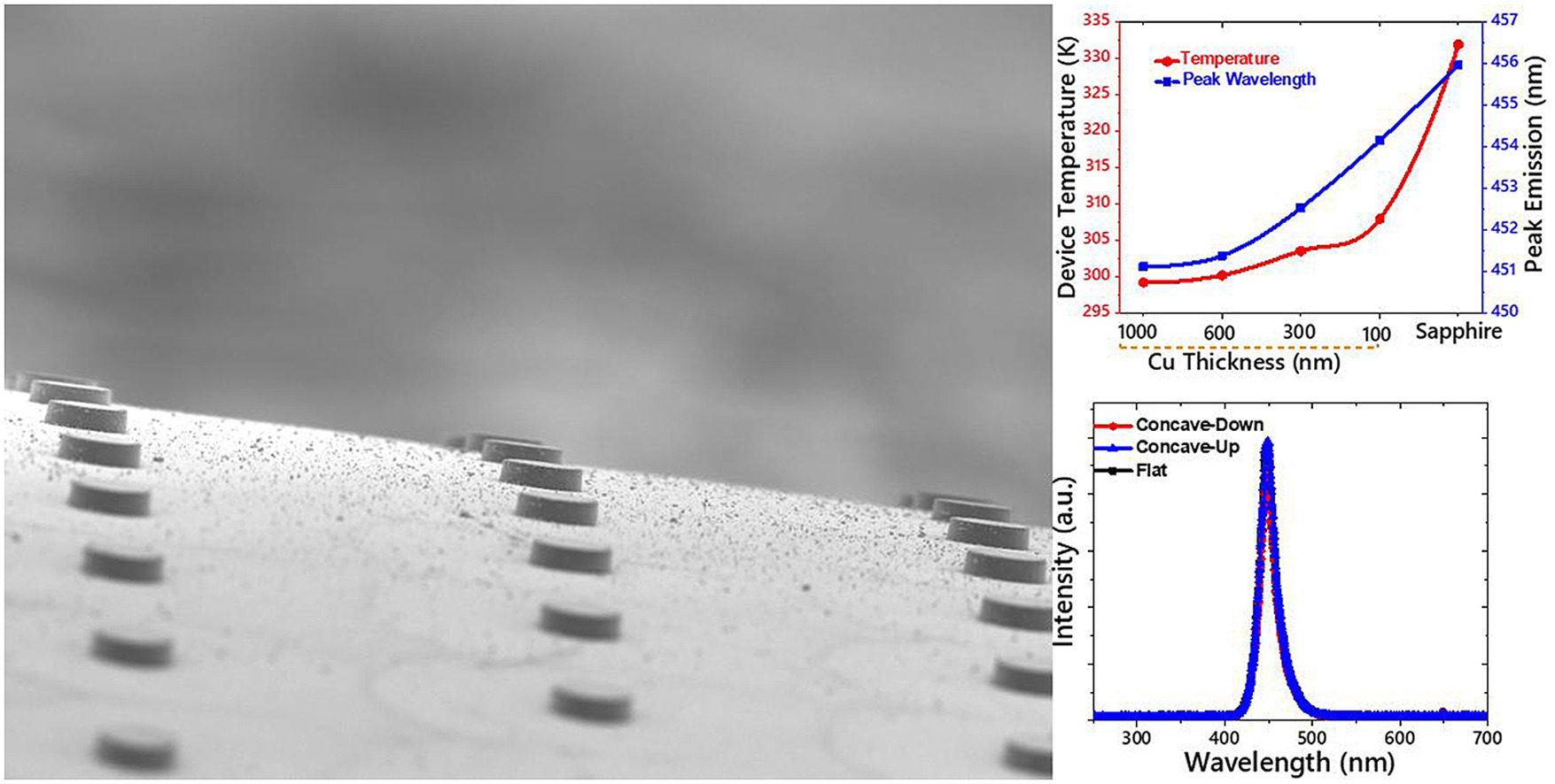
A Korean research team at Seoul National University designed a method to grow Micro LED on sapphire without etching process, which enables improved efficiency of Micro LED and improves transfer process.
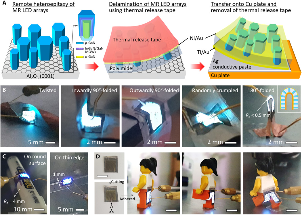
Another group of Korean researchers from Sejong University created a GaN Micro LED that is cuttable and foldable for easier transfer. The team manufactured Micro LEDs on a graphene-coated wafer by remote epitaxy. Given that the graphene surface does not chemically bond with the LED, the whole Micro LED is peeled off with an adhesive tape to form a panel. As a result, the LED can be freely deformed without breaking and the wafer can be reused repeatedly.

(Image: Sejong University)
Micro LED Transfer Technology Developments
Mass transferring is regarded as the most challenging process of Micro LED display production. Thus, many technology developers and researchers keep exploring the possible solution to improve the process. Several new approaches were introduced in the past few months.
A cross-country research team consisting of scientists from Taiwan’s NCTU, Yale University and Xiamen University, combined semipolar InGaN Micro LED with quantum dot photoresist to create full color Micro LED. In this way, mass transferring process for full color display could be simplified with only blue or UV LEDs required.
Researchers at the University of Waterloo in Canada presented a method, named “paste-and-cut,” to bond Micro LEDs on wafer onto a glass substrate and release them onto the flexible substrate. Based on the technique, the team developed a novel pixel circuit to compensate induced current degradation and achieved Micro LED chips of 20 µm without degradation.

(Image: University of Waterloo)
VerLASE, the Micro LED transferring technology supplier, introduced a novel transfer technology as well. The solution uses a novel formulation comprising of fab compatible chemistries and transfer stamp architecture in a unique way to deterministically pick-up a large number of microdies, translate them to the desired drop-off location on a substrate and then dispense them with very high accuracy and speed.
Micro LED Application Breakthroughs
In addition to technology progresses, LEDinside also learned several novel applications of Micro LED during COVID-19 pandemic.
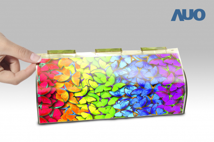
Panel maker AUO and Micro LED company PlayNitride jointly demonstrated a flexible Micro LED display in April this year. The 9.4-inch flexible Micro LED display featured a high resolution of 228 PPI achieved by more than 5.5 million Micro LEDs that are smaller than 30 µm.

(Image: AUO)
Apart from display application, many believe that Micro LED technology has a great potential in visible light communication as well. CEA-Leti announced their achievement in the field in June. The research institute used a 10 µm Micro LED to reach a data transmission rate of 7.7 Gbps.
Furthermore, Micro LED technology is also used in medical implant. Korea’s GIST introduced a Micro LED embedded medical implant system which supplies wireless power.
More Micro LED technology progresses and innovative applications will be revealed at 2020 Micro LED Forum. Industry professionals and technology builders will share their insights and latest findings of the emerging display technologies. Grasp your final chance for the early bird discount and register now.


