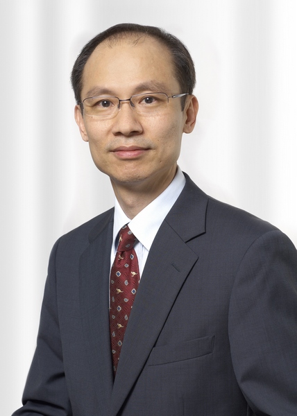
LEDinside recently interviewed Louis Lam CEO of Osram Opto Semiconductors Asia about the company’s future LED product outlook for niche market applications, including IR LED, laser diodes, and the automotive lighting market and German government subsidies that are supporting industry developments.
However, Lam declined to further comment on certain subjects, such as Osram’s decision to split its LED luminaire and traditional lighting ballast businesses.
 |
|
Louis Lam CEO of Osram Opto Semiconductors Asia. (All photos courtesy of Osram Opto Semiconductors) |
Q: What is the company’s future outlook for LED chip, package, IR LED,and laser diode businesses in terms of revenue growth?
In the second quarter of fiscal 2015, the Opto Semiconductors reporting segment recorded comparable revenue growth of 8% from a year earlier. All reporting regions contributed to this development. Growth was driven by the automotive, industrial and infrared business.
We see strong market demands and dynamics for the businesses of LED-based technologies and solutions.
Q: How did the InteGreat project come about?
This project has been started by the Germany Federal Government to develop a fully optimized production concept and process landscape for LED components and light modules. There all the process steps will be coordinated with one another and therefore could give rise to completely new types of LED and also reduce their manufacturing costs.
 |
|
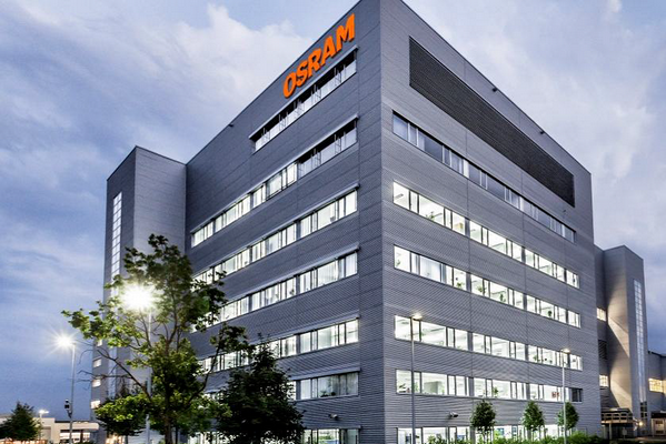
An Osram office. |
Q: What other LED or semiconductor subsidiaries has the German government issued to support developments in the LED industry?
The Germany government provides funding for novel technologies and process development addressing the societal challenges and supporting the leading position in of German technology-oriented companies. Due to their advantages of LED technology for lighting, there are several funding programs, where Osram participates with a variety of topics.
Q: Will the project cover LED chips and packaging technology?
The project will take a look into the production of high-efficiency LEDs along the entire production process. A holistic view of the manufacturing process – from epitaxy (crystal growth) to the light source itself – should enable synergies to be exploited for maximum effect and new approaches and procedures to be developed.
Q: How much LED chip manufacturing costs do you think can be reduced following this integrated manufacturing effort?
The objective of the recently started project is to develop innovative production concepts for high-efficiency LEDs. The project will run until 2017, after that the project results will be developed in a way to fit to state-of-the-art volume production concepts.
(Author: Judy Lin, Chief Editor, LEDinside)


