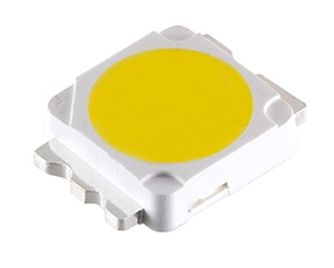
Toshiba Corporation will begin mass production of white LEDs on 200mm silicon wafers this month based on technology that it licensed and developed with Californian firm Bridgelux.
Deployment of Toshiba and Bridgelux’s gallium nitride-on-silicon (GaN-on-Si) technology to produce LED chips, has allowed Toshiba to replace sapphire substrates and produce the chips on a more cost-competitive silicon substrate.
Production of LED chips is typically done on two to four-inch wafers with an expensive sapphire substrate but Toshiba and Bridgelux have developed a process for manufacturing gallium nitride LEDs on 200mm silicon wafers, which Toshiba has brought to its new production line at Kaga Toshiba Electronics Corporation, a discrete products factory in northern Japan.

Toshiba expects to begin production this month of its first white LED silicon wafer product, the TL1F1 1W LED, which it says will deliver 112 lm at 350-mA drive current. The company plans to produce 10 million units per month.
The company will start sales of white LED packages to offer general and industrial OEMs what it claims will be a cost-competitive alternative to current LED solutions.
In a statement, Toshiba said: “The low power consumption and long life of white LED lighting is winning wide adoption in general purpose lighting, TV backlighting and other areas of application. In the 2011 financial year, the global market stood at 700 billion yen (£5.2 billion) and it is expected to almost double to 1,250 billion yen (£9.3 billion) in 2016 financial year. Going forward, Toshiba will promote product development and global sales toward securing a 10 per cent share of the world market in 2016.”
Last year, Bridgelux said it had successfully used silicon wafers to make commercial-grade LED components for the first time and that it had produced GaN-on-Si LEDs in the lab with an efficacy of 150 lm/W. It claims there is a potential 75 per cent improvement in cost when comparing silicon wafers with current LED manufacturing costs.


