Plessey Semiconductors announced today that it will be leading a GBP 1.3 million (US $2.01 million) government funded project in conjunction with AIXTRON and Bruker Nano Surfaces Division. This project will accelerate high volume manufacturing of Plessey’s innovative LEDs created with GaN-on-Silicon technology at its Devon based manufacturing site.
 |
|
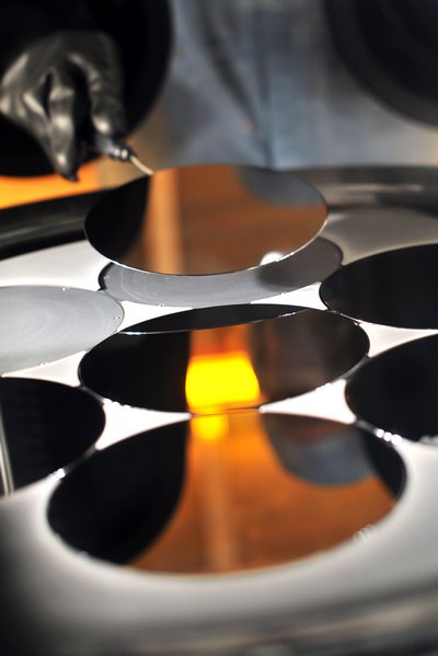
Plessey's GaN-on-Si wafers. (All photos courtesy of Plessey) |
In accordance with a press release issued on 26th March 2015 from the UK department for Business, Innovation and Skills, twenty supply chain projects from across the country will benefit from a total of £67 million of government investment. There is GBP109 million being invested in the same projects by industry.
Dr. Keith Strickland, Plessey CTO, said, “This project supports the work we have ongoing with AIXTRON and Bruker to further increase the yield of our GaN-on-Silicon process. These improvements are required as part of our move to 200mm (8-inch) silicon substrates. A 200mm (8-inch) wafer has almost twice the usable area of our existing 150mm (6-inch) wafers and therefore will almost double the number of LEDs produced for the same relative cost.”
 |
|
Dr. Keith Strickland, Plessey CTO. |
Plessey’s MaGIC™ (Manufactured on GaN-on-Silicon I/C) High Brightness LED (HBLED) technology has won numerous awards for its innovation and ability to cut the cost of LED lighting by using standard silicon manufacturing techniques. For further information and datasheets, please visit www.plesseysemiconductors.com or email enquiries@plesseysemi.com.


