 2019-09-20
Fine pitch display is becoming a trend in the panel market with more and more manufacturers developing advanced display products and technology solutions. GaN-on-Si Micro LED specialist Plessey announced that it has produced a record-breaking 2.5-micron pixel pitch ultra-high resolution Micro LED display for AR/VR wearable applications.
Plessey created an ultra-fine, ultra-high resolution 2000×2000 pixel display on a 2.5 microns pitch with its propriety monolithic GaN-on-Si technology. The UK-based company is dedicated to embedded Micro LED technology for...
Continue reading →
 2019-09-18
Plessey, the UK-based optoelectronic technology solutions developer, said that it has transferred its business focus from high-powered solid-state lighting, horticultural lighting and healthcare/ safety sensors sector to GaN-on-Si monolithic Micro LED display technology. The company is disrupting the global display market with a new generation of Augmented Reality (AR) devices and display solutions based on the Micro LED technology.
(Image: Plessey)
Featured with high brightness, high contrast, lower power consumption, fast refresh time and the capabilities of int...
Continue reading →
 2019-06-06
Plessey, the UK-based semiconductor technology provider, has successfully developed GaN-on-Si monolithic Micro LED. According to the company, the innovative development will support next generation applications such as AR headsets, head-up displays (HUD) and other smart wearables to enter the mass market.
Given their high contrast, high speed, wide viewing angle, high brightness and more efficient and longer-lasting operation, Micro LEDs are perfect for display applications on wearables such as smart watches, HUDs and AR headsets.
(Image: Plessey)
Howeve...
Continue reading →
 2018-12-14
ALLOS Semiconductor, the Germany-based IP licensing company, has announced its technology to avoid carbon-doping enable excellent performance of GaN-on-Si wafer as confirmed by the date of its customers. In an invited talk at the E-MRS scientific conference in Warsaw ALLOS’ co-founder and CTO Dr. Atsushi Nishikawa showed this data and the underlining analysis.
Being able to make this proof is important for the high power electronics (HPE) industry because it confirms the widespread believe that the absence of C-doping can help reduce switching los...
Continue reading →
 2018-11-13
UK-based Micro LED producer Plessey has announced a partnership with EV Group (EVG), a wafer bonding and lithography equipment supplier. The aim of the collaboration is to accelerate the commercialization of GaN-on-Si monolithic Micro LED technology.
Continue reading →
 2018-11-09
Veeco Instruments and ALLOS Semiconductors have continued their collaboration in developing GaN-on-Si epitaxy wafer for Micro LED production. The two companies have partnered to demonstrate the reproducibility of ALLOS’ 200 mm GaN-on-Si epitaxy wafer technology on Veeco’s Propel® MOCVD reactor.
“To bring Micro LED technology into production, simply presenting champion values for a single metric is insufficient. It is essential to achieve the whole set of specifications for each wafer with excellent repeatability and yield,” ...
Continue reading →
 2017-05-16
EpiGaN n.v., a worldwide provider of III-nitride epitaxial material solutions for advanced semiconductor manufacturing, will showcase the latest enhancements of its Gallium Nitride on Silicon epi-wafer family that meets industrial specifications for HEMT (High Electron Mobility Transistor) devices at 650V at PCIM Europe 2017 in Nuremberg, Germany, (May 16- 18, 2017) as ell as at CSMantech in Indian Wells, California, USA (May 22-14, 2017).
Continue reading →
 2016-01-19
The collaboration, which is partly funded by Innovate UK under the £14m Energy Catalyst Programme, follows on from work by Anvil Semiconductors and the Cambridge Centre for GaN at the University of Cambridge where they successfully grew cubic GaN on 3C-SiC on silicon wafers by MOCVD. The underlying 3C-SiC layers were produced by Anvil using its patented stress relief IP that enables growth of device quality silicon carbide on 100mm diameter silicon wafers.
Continue reading →
 2015-09-23
Plessey announced that it has developed a patented technology for Chip Scale Optics (CSO) based on its award winning GaN-on-Silicon MaGIC ™ LEDs. Chip Scale Optics permits design of light emission angles down to ten degrees direct from the LED. Having the primary optics on-chip eliminates the cost of primary optics typically found in packaged LEDs and chip-on-board modules. Furthermore, it significantly lowers the cost and provides for far greater design freedom for secondary optics within a luminaire. The first off applications include retail spot lighting, hospitality lighting, high and low bays, street lighting and stadium lighting. It is estimated that Plessey’s chip scale optics will halve the cost of these lighting applications.
Continue reading →
 2015-09-14
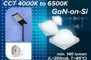
Toshiba Electronics Europe has added four new products to its TL1L4 series of white LEDs. These new additions provide a high luminous flux and are suited to applications ranging from street and stadium lighting to LED light bulbs and down lighting for use in the home.
Continue reading →
 2015-07-14
Plessey Semiconductors announced today that it will be leading a GBP1.3 million government funded project in conjunction with AIXTRON and Bruker Nano Surfaces Division. This project will accelerate high volume manufacturing of Plessey’s innovative LEDs created with GaN-on-Silicon technology at its Devon based manufacturing site.
Continue reading →
2015-06-24
Exagan, a start-up innovator of gallium-nitride (GaN) semiconductor technology that enables smaller and more efficient electrical converters,announced it has raised €5.7 million (US $6.38 million) in first-round financing that will be used to produce high-speed power switching devices on 200mm wafers.
Continue reading →
 2015-04-21
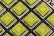
Plessey Semiconductors announced it will be featured in a new website showcasing 21st century British manufacturing which will be launched 23rd April at a high-profile event in London.
Continue reading →
 2015-04-02
Leading LED chip industry experts had very different perspectives on GaN LED substrates at 2015 LED Executive Summit hosted by SEMI at TILS 2015 in TWTC Nangang Exhibition Hall, Taipei, Taiwan recently.
Continue reading →
2015-03-30
Shunfeng International Clean Energy Limited (SFCE) announced that it has signed an MOU with Lattice Power to acquire a 51% ownership stake in the company. SFCE's successful bid in Lattice Power is a milestone for the listed company as it transitions to become a global low carbon solutions provider. Lattice Power's gallium nitride (GaN) on silicon technology is exclusively patented worldwide, offering significant cost advantages compared to sapphire substrate technology LED. The partnership expands SFCE's portfolio and increases the profitability of the listed company.
Continue reading →
2015-03-19
Infineon Technologies announced the expansion of its Gallium Nitride (GaN)-on-Silicon technology and product portfolio. The company now offers both enhancement mode and cascode configuration GaN-based platforms optimized for high performance applications requiring superior levels of energy efficiency including Switch Mode Power Supplies (SMPS) used in server, telecom, mobile power and consumer goods such as Class D Audio systems. GaN technology significantly reduces the size and weight of power supplies which will open up new opportunities in end-products such as ultra-thin LED TVs.
Continue reading →
 2015-03-16
Leading Taiwanese LED maker Epistar announced recently that the company had acquired German manufacturer ALLOS unique GaN-on-Si technology. ALLOS has licensed the related patent to Epistar, and the two companies have concluded the initial phase of its technology transfer project. For further information please see original press release below.
Continue reading →
2015-01-12
The main objective of Epistar’s acquisition of TSMC SSL is to obtain key LED substrate technology to prevent Japanese manufacturer Toshiba from taking the lead in GaN-on-Si technology, according to a Chinese-language Wealth Magazine report.
Continue reading →
 2014-06-04
LatticePower, will display at LIGHTFAIR International 2014 (booth #1933B) the next generation of light fixtures demonstrating the true convergence of performance, design and affordability. The company's new proprietary GaN-on-Silicon LED track, highbay and flood fixtures deliver outstanding efficacy, superior brightness and excellent color rendering.
Continue reading →
2014-05-08
LED chips are a core component in the LED industry. There are currently many domestic and international LED chip manufacturers in China, but there currently are no categorization standards, according to a report by Chinese-language LEDtimes.cc. Comparison of chip technologies show foreign companies are more innovative, while Chinese manufacturers are still focused on production volume.
Continue reading →
 2014-03-26
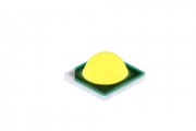
Toshiba Corporation announced the launch of two new series of white LEDs, the 3.5 x 3.5mm lens package 1W type “TL1L2 series,” and the 3.0 x 3.0mm flat package 0.6W type “TL3GB series”. Mass production of both will start from the end of March.
Continue reading →
 2013-10-29
Toshiba Electronics Europe (TEE) has announced the first devices in its second generation of LETERAS white LEDs fabricated using a gallium nitride-on cilicon (GaN-on-Si) process. The 1W TL1F2 LEDs offer a cost-competitive alternative to current LED packages, allowing manufacturers of general purpose and industrial LED lighting to drive down costs.
Continue reading →
 2013-03-13
AIXTRON SE announced that US company Transphorm Inc. is stepping up production of gallium nitride on silicon (GaN-on-Si) with its latest order of AIXTRON’s G5+ MOCVD system, capable of handling five 200 mm (5x8-inch) wafers. The order was made in the fourth quarter of 2012 with delivery due in the second quarter of 2013. Primit Parikh, President of Transphorm comments: “We are not just increasing our capacity with this order. This new system also expands our capability from 150 mm to 200 mm diameter wafers, providing economies of scale. We ...
Continue reading →
 2013-03-06
AIXTRON SE has been awarded the 2013 Compound Semiconductor Manufacturing Award for its latest development, the AIX G5+ reactor for gallium nitride on silicon (GaN-on-Si). The Award recognizes key areas of innovation surrounding the chip manufacturing process from research to completed device, focusing on the people, processes and products that drive the industry forward. Editor Richard Stevenson from Compound Semiconductor (CS) magazine presented the award yesterday, March 4, 2013 to AIXTRON’s Vice President Europe Dr. Frank Schulte. &...
Continue reading →
2012-09-14
The easy migration of LED manufacturing to GaN-on-Si is described in a White Paper released by AZZURRO. Utilizing the company’s 150 mm templates the advantages of GaN-on-Si can be gained after very short design-in times. The White Paper outlines technical hurdles to be overcome when migrating to GaN-on-Si, covers key achievements possible when using the right technology, details the advantages for the move to GaN-on-Si obtainable with templates and shows development solutions to the LED epitaxy engineer. In detail data of GaN-on-Si products is rev...
Continue reading →
2012-08-14
AIXTRON SE today announced a new MOCVD system order from National Central University (NCU) in Taiwan. Existing customer, NCU has placed an order for one 1x6-inch AIXTRON Close Coupled Showerhead MOCVD system, which will be dedicated to the growth of GaN epitaxial structures on 6-inch silicon substrates, for use in the research and development of power management devices. AIXTRON’s local support team has installed and commissioned the new reactor in the state-of-the-art cleanroom facility at NCU’s Microwave and Optoelectroni...
Continue reading →
 2019-09-20
 2019-09-18
 2019-06-06
 2018-12-14
 2018-11-13
 2018-11-09
 2017-05-16
 2016-01-19
 2015-09-23
 2015-09-14
 2015-07-14
 2015-04-21
 2015-04-02
 2015-03-16
 2014-06-04
 2014-03-26
 2013-10-29
 2013-03-13
 2013-03-06