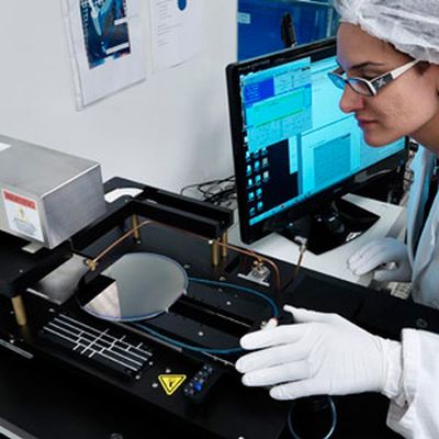
EpiGaN n.v., a worldwide provider of III-nitride epitaxial material solutions for advanced semiconductor manufacturing, will showcase the latest enhancements of its Gallium Nitride on Silicon epi-wafer family that meets industrial specifications for HEMT (High Electron Mobility Transistor) devices at 650V at PCIM Europe 2017 in Nuremberg, Germany, (May 16- 18, 2017) as ell as at CSMantech in Indian Wells, California, USA (May 22-14, 2017). At PCIM Europe 2017, EpiGaN will exhibit in Hall 6, Booth 432.
(Image: EpiGaN)
Drawing on its leading technology position in advanced GaN-on-Si and GaN-on-SiC materials for highperformance power switching and RF power devices for millimeter-wave applications, EpiGaN is leading the way to define epi-wafer material quality for device properties that cut conversion losses and increase reliability. With its cost-efficient GaN-on-Si technology, EpiGaN has enabled path braking innovations in 650V power management and RF power systems, such as scaling GaN/Si technology up to 200mm for economies of scale to enter the mainstream CMOS manufacturing lines of Si-based IDMs and foundries.
EpiGaN has taken up and successfully mastered this manufacturing challenge and developed 200mm versions of its HV650V and HVRF GaN-on-Si epiwafers. Among the distinctive achievements of EpiGaN's HV650V RF power products are good dynamic behavior for power devices and lowest RF losses (<0.5dB/mm up to 50GHz) for the HVRF product family.
An important competitive advantage and key concept of EpiGaN's GaN/Si epi-wafer technology is the in-situ SiN capping layer. This special feature, as pioneered by EpiGaN, provides superior surface passivation and device reliability, and it enables the contamination-free processing in existing standard Si-CMOS production infrastructures. In-situ SiN structuring also allows the use of pure AlN layers as barrier materials, which results in lower conduction losses and/or allows the design of smaller-size chips for the same current rating.
"GaN technology has begun to enter many applications, either in power switching or in RF power amplification," says EpiGaN cofounder and CEO Dr Marianne Germain. "We supply industry-leading 200mm GaN-on-Si epi-wafers to the global semiconductor industry, and we are particularly proud to have developed GaN-on-Si epi-wafers that show the lowest RF loss up to 100GHz. This is a timely answer to the increasing demands in wireless communication such as the introduction of 5G and the Internet of Things."
At PCIM Europe, Dr Germain will participate in a high-ranking panel discussion "GaN - Design, EMC and Measurement" at the Fach Forum, organized by Bodo’s Power Systems (May 17). Dr Markus Behet, EpiGaN CMO, will give a presentation entitled “From Hype to Reality: GaN/Si - Where Are We Today?” at the PCIM Europe Exhibitor Forum (May 18) and the CSMantech Exhibitor Forum (May 23).


