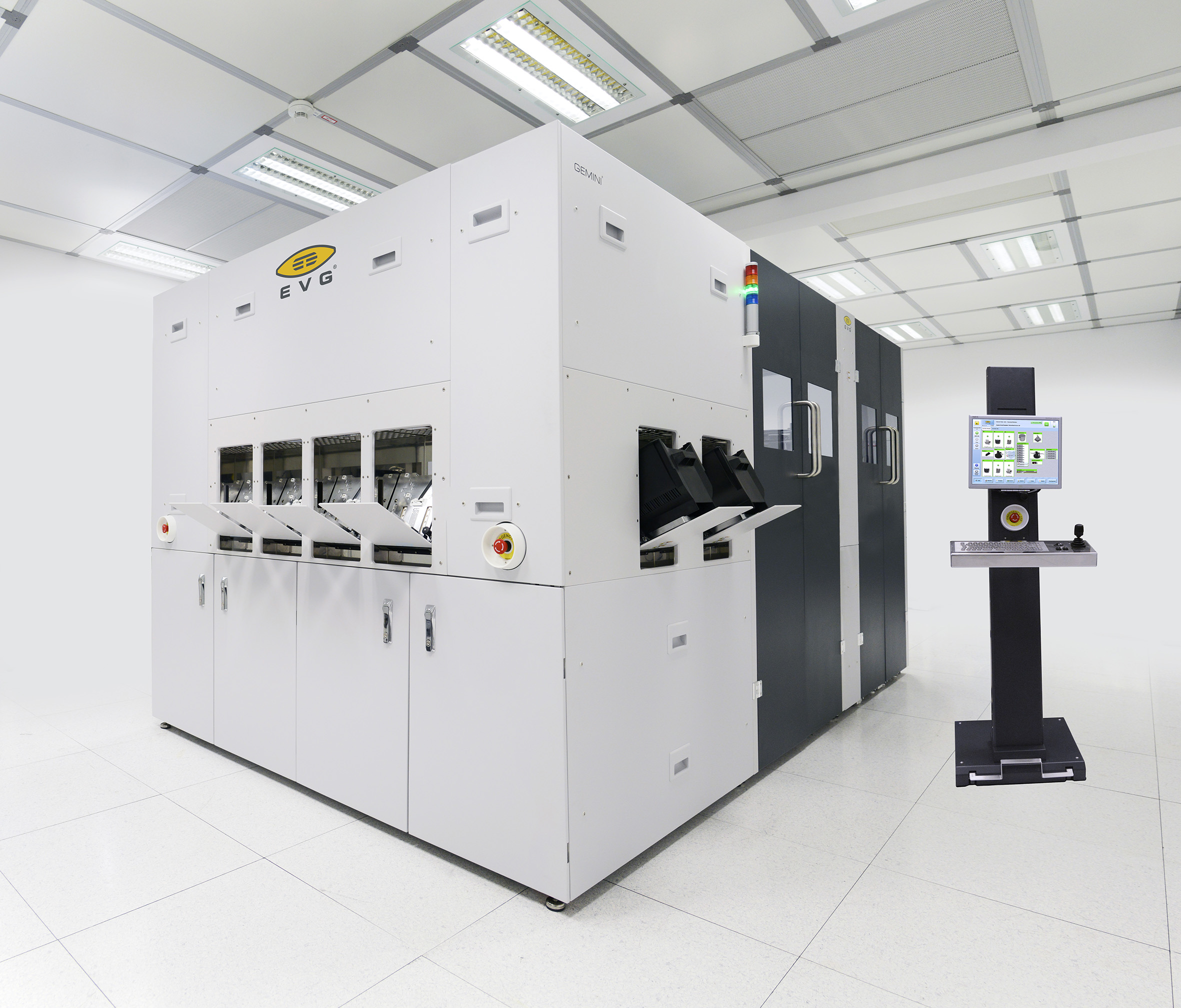
UK-based Micro LED producer Plessey has announced a partnership with EV Group (EVG), a wafer bonding and lithography equipment supplier. The aim of the collaboration is to accelerate the commercialization of GaN-on-Si monolithic Micro LED technology.

(Image: Plessey)
Plessey has purchased a GEMINI® production wafer bonding system from EVG to bond and align its GaN-on-Si Micro LED arrays to the panel’s backplane at a wafer level. As the size of Micro LED is very small, EVG’s SmartView®NT Automated Bond Alignment System technology can achieve a high level of alignment precision that is necessary for small pixel dimensions. Moreover, EVG’s equipment allows face-to-face alignment of the wafers and a maximum level of automation and process integration, enabling wafer bonding processes up to 300mm for volume manufacturing.
“The modular design of the GEMINI system is ideal for our requirements. Having the pre-treatment, clean, alignment and bonding enabled within one system means higher yield and throughput in production. The excellent service provided by EVG has been critical to bringing the system online quickly and efficiently,” said, John Whiteman, VP of Engineering at Plessey.
Plessey has continued to accelerate its GaN-on-Si monolithic Micro LED technology development and targeted AR applications. The company unveiled its collaboration with Vuzix for developing advanced Micro LED display for AR smart glasses in June. In September, Plessey also announced a partnership with Jasper Display for silicon backplane and selected Aixtron’s MOCVD system for its Micro LED wafer production.


