 2018-11-13
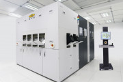
UK-based Micro LED producer Plessey has announced a partnership with EV Group (EVG), a wafer bonding and lithography equipment supplier. The aim of the collaboration is to accelerate the commercialization of GaN-on-Si monolithic Micro LED technology.
Continue reading →
 2017-11-14
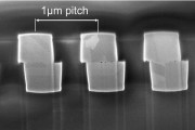
EV Group and Leti completed the world's first successful 300-mm wafer-to-wafer direct hybrid bonding with pitch dimension connections as small as 1µm (micron).
Continue reading →
 2017-09-12
EV Group (EVG), a supplier of wafer bonding and lithography equipment for the MEMS, nanotechnology and semiconductor markets, announced it has received multiple orders for its comprehensive portfolio of manufacturing equipment and services designed to address the burgeoning demand for wafer-level optics (WLO) and 3D sensing.
Continue reading →
 2016-03-15
New EVG®7200 LA SmartNIL™ system brings high-resolution and low cost-of-ownership advantages to high-end displays, photonics, optics and biotechnology applications.
Continue reading →
 2015-08-26
EV Group (EVG), a leading supplier of wafer bonding and lithography equipment for the MEMS, nanotechnology and semiconductor markets, will host a special session at the 41st Micro and Nano Engineering (MNE 2015) conference--a leading international conference on micro- and nanofabrication and manufacturing using lithography and related techniques. The first EVG Photonics Workshop will take place at the World Forum in The Hague, The Netherlands, during the afternoon of the opening day of MNE 2015 on Wednesday, September 21.
Continue reading →
 2015-07-08
EV Group (EVG), a leading supplier of wafer bonding and lithography equipment for the MEMS, nanotechnology and semiconductor markets, today unveiled the HERCULES® NIL—a fully integrated track system that combines cleaning, resist coating and baking pre-processing steps with EVG's proprietary SmartNIL™ large-area nanoimprint lithography (NIL) process in a single platform. Offering industry-leading productivity and throughput, the HERCULES NIL provides a complete, dedicated UV-NIL solution that is ideally suited for high-volume manufacturing (HVM) of emerging photonic devices.
Continue reading →
 2012-02-08
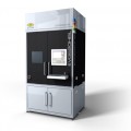
Updated HB-LED Manufacturing Tool Commands Unprecedented Cost of Ownership Advantages EV Group (EVG), a leading supplier of wafer-bonding and lithography equipment for the advanced semiconductor and packaging, compound semiconductors, MEMS, silicon-on-insulator (SOI) and emerging nanotechnology markets, today announced the EVG620HBL Gen II—the second generation fully automated mask alignment system for volume manufacturing of high-brightness light-emitting diodes (HB-LEDs). Introduced one year after the launch of the first-generation E...
Continue reading →
2012-01-11
Eulitha AG, a pioneer and leader in the production of high-quality nanostructures using advanced lithography techniques, today announced that it has signed a joint-development and licensing agreement with EV Group (EVG), a leading supplier of wafer bonding and lithography equipment for the MEMS, nanotechnology and semiconductor markets. EVG will integrate Eulitha’s PHABLE™ mask-based ultraviolet (UV) photolithography technology with EVG’s automated mask aligner product platform with the goal of developing a low-cost-of-ownership (CoO) nanopatte...
Continue reading →
 2018-11-13
 2017-11-14
 2017-09-12
 2016-03-15
 2015-08-26
 2015-07-08
 2012-02-08