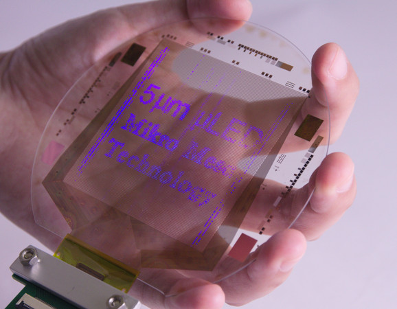
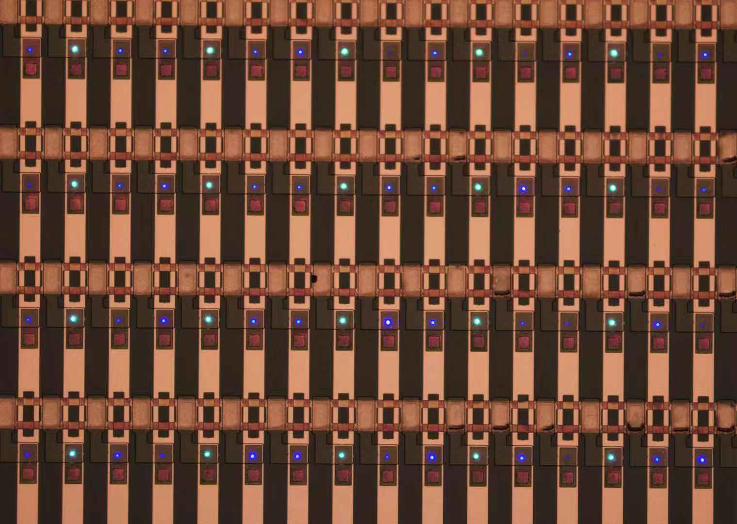
Mikro Mesa Technology announced a breakthrough in Micro LED mass transferring and bonding which successfully transferred Micro LED chips sized 3µm to manufacture a 4-inch display.

(Image: Mikro Mesa)
Mikro Mesa’s technology is capable of transfer chips sized 2 to 5 µm with large transfer stamp size (close to 4 inches) which would reduce transfer counts and the cycle time. By using the pick and place method, the mass transfer process can bond different color uLED chips and make a full color display.
The company also noted that the transfer technology can produce display with a resolution up to 1,800 dpi with millions of Micro LED chips, enabling large size applications including TVs above 55-inch. In addition, the technology is featured with low temperature (below 200 degree Celsius) and pressure-free pitch bonding for better yield. The low temperature process also fits the requirements of flexible and transparent display production.

(Image: Mikro Mesa)
Vertical structured Micro LEDs are used in Mikro Mesa’s proprietary manufacture process. According to Mikro Mesa, the structure allows the current distributed more evenly compared to flip-chip structure and supports higher input.
Mikro Mesa Technology was established in 2014 by Dr. Li-Yi Chen for Micro LED technology development. The company has worked with China Electronics Panda on Micro LED since 2017 and announced its technology breakthrough for the next generation display technology. Mikro Mesa believes that this technology progress plays a key role for Micro LED commercialization. Currently the company owns a patent portfolio of 36 U.S. granted patents and more than 100 pending world patents.
Chen said, "This elegant technology will help Micro LED display to eliminate the cost obstacle to enter the consumer market which is dominated by OLED and LCD today. Because of the tiny chip size, the material cost can be reduced much further. That makes the uLED display can compete with OLED even LCD in the future."


