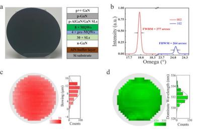
Researchers from Hunan University have designed and grown wafer-scale uniform green GaN epilayer on silicon wafers (4-inch and 6-inch in size). The epilayer was of very high uniformity and showed excellent properties. Using this wafer, the researchers developed green microLED displays reaching over 10 million nits.

This epilayer demonstrated a low dislocation density of 5.25×108 cm-2, minimal wafer bowing of 16.7 μm, and high wavelength uniformity (STDEV<1 nm). The researcher integrated the Micro-LEDs with CMOS circuits and created 1080x780 monochrome green microLED displays, which offered the ultra high brightness.
To achieve the high performance epilayer, the researchers used gallium (Ga)-assisted method for AlN growth, to address the challenges of low-temperature preparation of high-quality AlN buffer layers on silicon substrates. In addition, the researchers created a highly controllable roughening process combined with atomic-level sidewall passivation treatment to overcome the bottleneck in microLED luminous efficiency. Another technique the researchers developed was vertical non-alignment bonding, which allows for the seamless integration of the display with the CMOS driver.
TrendForce 2024 Micro LED Market Trend and Technology Cost Analysis
Release: 31 May / 30 November 2024
Language: Traditional Chinese / English
Format: PDF
Page: 160-180
|
If you would like to know more details , please contact:
|


