 2026-04-27
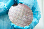
Recently, China-based Ziener Tech has unveiled progress in sapphire substrate thinning, announcing that it has successfully reduced the substrate thickness of its 8-inch GaN-on-sapphire wafers to 50μm. In practical applications, heat dissipation has long been a key bottleneck limiting GaN device performance. Substrate material plays a critical role in thermal management. Sapphire offers strong insulation, high thermal stability, and relatively good lattice and thermal matching with GaN, enabling simpler epitaxial structures. However, its inherently low thermal conducti...
Continue reading →
 2025-07-04
As TSMC doubles down on advanced node development to ride the AI wave, it’s steadily pulling back from legacy businesses. According to the Commercial Times, citing a press release from Navitas Semiconductor, TSMC will wind down its Gallium Nitride (GaN) wafer foundry services by July 31, 2027. Notably, ijiwei suggests that TSMC plans to repurpose its Hsinchu Fab 5, currently used for GaN, for advanced packaging starting July 1, 2025. By reusing existing cleanroom facilities, TSMC can accelerate expansion with minimal effort—a timely move ...
Continue reading →
 2024-10-25
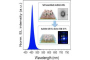
Researchers from Korea's Kookmin University in collaboration with colleagues from Kyung Hee University have managed to enhance the performance of microLEDs produced using fluidic self-assembly based on chelation bonds of chemical linkers. The researcher report up to 61.8% increase in assembly yield compared to previous methods, and their vertically assembled 1.3 um microLEDs achieved a peak EQE of 8.1% and a brightness of 22,300 nits at 9 V.
The researcher developed a novel approach for the face-selective vertical assembly of microLEDs using a chemical linker c...
Continue reading →
 2024-10-25
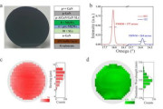
Researchers from Hunan University have designed and grown wafer-scale uniform green GaN epilayer on silicon wafers (4-inch and 6-inch in size). The epilayer was of very high uniformity and showed excellent properties. Using this wafer, the researchers developed green microLED displays reaching over 10 million nits.
This epilayer demonstrated a low dislocation density of 5.25×108 cm-2, minimal wafer bowing of 16.7 μm, and high wavelength uniformity (STDEV<1 nm). The researcher integrated the Micro-LEDs with CMOS circuits and created 1080x780 monochrom...
Continue reading →
 2024-10-09
Project with Macquarie University and Aurizn will develop ocean LiDAR for measuring subsurface water temperature and depth Semiconductor developer Blugass has signed an agreement with Macquarie University and defence company Aurizn to develop and test a new laser-based method to measure subsurface water temperature and depth. BluGlass will provide high-power multi-transverse-mode GaN lasers to the 12-month blue ocean LiDAR project, partially funded by an Australia's Economic Accelerator (AEA) Seed Grant, to support the commercialisation of visible lase...
Continue reading →
 2022-12-07
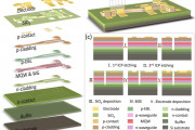
Researchers in China and Japan have demonstrated a monolithic gallium nitride (GaN) optoelectronic system on silicon (Si) substrate consisting of a transmitter, modulator, waveguide, beam splitter, receivers and monitor [Hao Zhang et al, Appl. Phys. Lett., v121, p181103, 2022].
The team from China’s Nanjing University of Posts and Telecommunications and Zhengzhou University and Japan’s Nagoya University are seeking to promote optoelectronic systems with low power consumption while using monolithic integration on silicon to reduce material, pr...
Continue reading →
2022-11-28
BluGlass has signed a paid development agreement with Ganvix, Inc - a leading developer of GaN Vertical Cavity Surface Emitting Lasers (VCSELs) Ganvix has selected BluGlass’ RPCVD technology to enable the development of green VCSELs for advanced applications Global semiconductor developer BluGlass Limited (ASX: BLG) has entered into a collaboration agreement with Ganvix, Inc. to develop cutting-edge gallium nitride (GaN) vertical cavity surface emitting lasers (VCSELs) for green wavelengths (515nm-525nm). Ganvi...
Continue reading →
 2021-10-05
GaN, the “Black Technology” in the compound semiconductor market, can largely reduce product size thanks to its high power and high density. The compound also maintains excellent properties under high-frequency, high-temperature and high-voltage circumstances. The increasing demand for GaN in 5G/6G, renewable energy and electric vehicle markets will boost the material’s value in the context of consumer electronics and related industrial chains. GaN is going to be the next-gen “superstar” in the semiconductor industry.
The Department of Industri...
Continue reading →
 2021-09-03
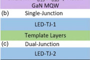
Ohio State University and Sandia National Laboratories in the USA claim the first demonstration of triple-junction cascaded III-nitride light-emitting diodes (LEDs) grown by metal-organic chemical vapor deposition (MOCVD) [Zane Jamal-Eddine et al, Appl. Phys. Express, v14, p092003, 2021]. Stacking LEDs is one way to overcome the limitations in output power density imposed by the effects of efficiency droop at large current density. Tunnel-junction (TJ) structures are used to connect LEDs since they enable electron majority carriers to be transformed to ...
Continue reading →
 2021-06-28
Some of the advantages of third-generation semiconductors SiC and GaN include their ability to operate under high voltages, high temperatures (for SiC), and high frequencies(for GaN). Not only do these advantages allow manufacturers to significantly reduce the physical sizes of chips, but peripheral circuit designs can also be simplified as a result, thereby further reducing the sizes of modules, peripheral components, and cooling systems. That is why SiC and GaN have become important strategic focuses of the global semiconductor industry.
As part of its ongoing goa...
Continue reading →
 2021-06-15
In response to the increasing demands of mobile applications, manufacturers are now placing a priority on extending the battery life of such devices like smartphones and notebook computers. However, due to the inherent limitations of physical space in these devices, the quest for ever-greater battery capacity has seemingly reached a bottleneck, forcing them to look elsewhere for solutions, hence the development of fast charging technology. As such, fast chargers equipped with GaN (Gallium nitride, which is a third-generation semiconductor) chips have are now expected to introduce th...
Continue reading →
 2020-11-24
World first is set to transform next-generation display technology.
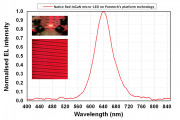
University of Cambridge spin-out Porotech has today announced the launch of its first product based on its breakthrough gallium nitride (GaN) production technique that is set to transform the electronics industry. The company has launched the world's first commercial native red LED epiwafer for micro-LED applications.
Micro-LED display technology offers a huge improvement on standard display panels due to its optimum brightness, efficiency and image definition, as well as improved lifetime. These b...
Continue reading →
 2020-04-09
Poro Technologies (Porotech), is a spin-out from the University of Cambridge focusing on GaN material technology. The company has closed a GBP 1.5 million (US$ 1.86 million) seed round investment.
According to the report of Cambridge, the investment will support Porotech to develop a pilot plant in Cambridge and its first major products. The seed round was co-led by Cambridge Enterprise, the commercialization arm of the University of Cambridge, and IQ Capital Partners, with the additional participation of Martlet Capital and a syndicate of angel investors from ...
Continue reading →
 2020-02-21
STMicroelectronics announced the collaboration with TSMC to accelerate the development of Gallium Nitride (GaN) process technology and the supply of both discrete and integrated GaN devices to market. Through this partnership, ST’s GaN products will be manufactured using TSMC’s GaN process technology.
GaN is a wide bandgap semiconductor material which is considered outpacing traditional Silicon-based semiconductors for power applications. GaN is more energy efficient at high power and allows the design of more compact devices for better form fact...
Continue reading →
 2019-07-04
German semiconductor equipment provider AIXTRON announced its partnership with Nagoya University in Japan. The equipment maker has delivered a Close Coupled Showerhead® (CCS) system to the University’s Institute of Materials and Systems for Sustainability (IMaSS).
AIXTRONs 3x2-inch Flip Top CCS MOCVD platform is intended for research in the field of GaN-based deep ultra-violet (DUV) optoelectronic devices. Specially designed for research and small series production, the AIXTRON system enables real scaling from R&D ...
Continue reading →
 2018-10-04
Dr. Hiroshi Amano, a 2014 Nobel laureate in physics, delivered a lecture at Academia Sinica, Taipei, Taiwan on October 3rd, sharing his research progress on GaN blue LED with Prof. Isamu Akasaki and how he has transferred his research focus from blue LED to UV LED and GaN power. He also highlighted the potential applications of GaN technology in the era of IoT and 5G.
Continue reading →
 2018-09-11
SEMICON Taiwan 2018 was held at Taipei Nangang Exhibition Center on September 5 -7. Many leading equipment manufacturers have joined the event including Aixtron, Veeco, Kulicke & Soffa, MPI Corporation and Toray. These equipment makers have introduced the latest trends of power components and optoelectronic.
Continue reading →
 2016-12-08
Gallium nitride (GaN) has emerged as one of the most important and widely used semiconducting materials. Its optoelectronic and mechanical properties make it ideal for a variety of applications, including light-emitting diodes (LEDs), high-temperature transistors, sensors and biocompatible electronic implants in humans.
Continue reading →
 2016-11-21
German MOCVD manufacturer Aixtron and Chinese investor Grand Chip Investment are determined to complete the acquisition business transaction despite objections raised by the Committee on Foreign Investment in the United States (CFIUS).
Continue reading →
 2016-08-26
Ten years after launching a gallium nitride (GaN) semiconductor company, the two Ottawa-based co-founders of GaN Systems, President Girvan Patterson and CTO John Roberts have announced their retirement. Having achieved their goal of building GaN Systems into the world leading manufacturer of GaN power transistors and supplier to more than 500 customers, serial entrepreneurs Patterson and Roberts will leave their operating roles. Patterson will retain a position on GaN Systems’ Board of Directors, while Roberts will remain available to the company as an emeritus contributor.
Continue reading →
2016-08-18
Chinese manufacturers technology have advanced in the past year to result in large GaN price fluctuations, and have entered III-V EPI-wafer synthesizing industry to build a comprehensive IoT and telecommunication supply chain in the upstream sector.
Continue reading →
 2016-05-26
NXP Semiconductors N.V. (NASDAQ:NXPI), today announced an expansion to its portfolio of 48V Gallium Nitride (GaN) RF power transistors optimized for Doherty power amplifiers for use in current and next-generation cellular base stations. The four new transistors collectively cover cellular bands from 1805 to 3600 MHz, meeting the needs of wireless carriers for superior performance at higher frequencies.
Continue reading →
 2016-03-31
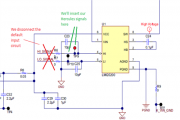
In my last blog post, I walked you through a hands-on project: dimming a lamp with a gallium nitride (GaN) power stage, a Hercules™ microcontroller and a scroll wheel. I covered setup, design and how to drive the power stage the right way.
Continue reading →
 2016-03-23
Sandeep Bahl of Texas Instrument stresses the importance of making reliable GaN material will largely rely on joint efforts in the industry to establish related standards in this blog entry.
Continue reading →
2016-02-17
Veeco Instruments Inc., the world’s leading supplier of metal organic chemical vapor deposition (MOCVD) systems, announced today that it has signed a joint development project (JDP) agreement with imec, the Belgium-based nano-electronics research center. The collaboration is expected to accelerate the development of highly-efficient, Gallium Nitride (GaN) based, power electronic devices using GaN Epi wafers created using Veeco’s Propel® Power GaN MOCVD system.
Continue reading →
 2016-01-13
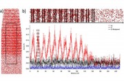
In the fabrication of solid state lighting devices, scientists are learning, oxygen also plays a two-edged role. While oxygen can impede the effectiveness of gallium nitride (GaN), an enabling material for LEDs, small amounts of oxygen in some cases are needed to enhance the devices' optical properties. GaN doped with europium (Eu), which could provide the red color in LEDs and other displays, is one such case.
Continue reading →
2015-07-13
Global semiconductor capital equipment manufacturer OEM Group announced today that a leading maker of LED products has placed a repeat order for an AGHeatpulse® RTP system. The system will be used for annealing gallium-nitride (GaN) films deposited on 150mm sapphire substrates, one of the critical process steps needed in advanced LED fabrication. This repeat order validates again the AGHeatpulse® RTP system's demonstrated capabilities meeting the exacting thermal requirements of new LED manufacturing technologies, and supports the LED industry's move from batch processing of smaller diameter sapphire substrates to single wafer processing of 150mm sapphire substrates.
Continue reading →
 2015-06-29
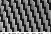
The latest research from the Niels Bohr Institute shows that LEDs made from nanowires will use less energy and provide better light. The researchers studied nanowires using X-ray microscopy and with this method they can pinpoint exactly how the nanowire should be designed to give the best properties. The results are published in the scientific journal, ACS Nano.
Continue reading →
 2015-03-23
You may have recently encountered “GaN,” which is replacing silicon (Si) in some key applications for power conversion. In this blog series, “How to design with GaN,” I will take a look at how gallium nitride (GaN) is different from Si and what the key considerations are when creating a power design with GaN.
Continue reading →
2015-02-12
Veeco Instruments announced that the Fraunhofer Institute for Applied Solid State Physics IAF, a leading German compound semiconductor research institution, has purchased a TurboDisc® K465i Gallium Nitride (GaN) MOCVD System.
Continue reading →
 2026-04-27
 2025-07-04
 2024-10-25
 2024-10-25
 2024-10-09
 2022-12-07
 2021-10-05
 2021-09-03
 2021-06-28
 2021-06-15
 2020-11-24
 2020-04-09
 2020-02-21
 2019-07-04
 2018-10-04
 2018-09-11
 2016-12-08
 2016-11-21
 2016-08-26
 2016-05-26
 2016-03-31
 2016-03-23
 2016-01-13
 2015-06-29
 2015-03-23