Gallium nitride (GaN) has emerged as one of the most important and widely used semiconducting materials. Its optoelectronic and mechanical properties make it ideal for a variety of applications, including light-emitting diodes (LEDs), high-temperature transistors, sensors and biocompatible electronic implants in humans.
In 2014, three Japanese scientists won the Nobel Prize in physics for discovering GaN’s critical role in generating blue LED light, which is required, in combination with red and green light, to produce white LED light sources.
Now, four Lehigh engineers have reported a previously unknown property for GaN: Its wear resistance approaches that of diamonds and promises to open up applications in touch screens, space vehicles and radio-frequency microelectromechanical systems (RF MEMS), all of which require high-speed, high-vibration technology.
 |
|
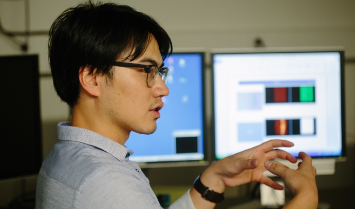
Ph.D. candidate Guosong Zeng is part of a Lehigh research group that was the first to explore the wear resistance of gallium nitride. Their discovery could have a dramatic effect on the electronic and digital device industries.(Photo courtesy of Christa Neu) |
The researchers reported their findings in August in Applied Physics Letters (APL) in an article titled “Ultralow wear of gallium nitride.” The article’s authors are Guosong Zeng, a Ph.D. candidate in mechanical engineering; Nelson Tansu, the Daniel E. ’39 and Patricia M. Smith Endowed Chair Professor in the electrical and computer engineering department and director of the Center for Photonics and Nanoelectronics (CPN); Brandon A. Krick, assistant professor of mechanical engineering and mechanics; and Chee-Keong Tan ’16 Ph.D., now assistant professor of electrical and computer engineering at Clarkson University.
GaN’s electronic and optical properties have been studied extensively for several decades, said Zeng, the lead author of the APL article, but virtually no studies have been done of its tribological properties, that is, its resistance to the mechanical wear imposed by reciprocated sliding.
“Our group is the first to investigate the wear performance of GaN,” said Zeng. “We have found that its wear rate approaches that of diamonds, the hardest material known.”
 |
|
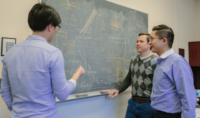
Zeng, with Brandon Krick (center) and Nelson Tansu, performed dry sliding wear experiments on gallium nitride coatings grown epitaxially with metalorganic chemical vapor deposition (MOCVD) on single crystalline sapphire wafers.(Photo courtesy of Christa Neu)
|
Wear rate is expressed in negative cubic millimeters of Newton meters (Nm). The rate for chalk, which has virtually no wear resistance, is on the order of 10-2 mm3/Nm, while that of diamonds is between 10-9and 10-10, making diamonds eight orders of magnitude more wear resistant than chalk. The rate for GaN ranges from 10-7 to 10-9, approaching the wear resistance of diamonds and three to five orders of magnitude more wear resistant than silicon (10-4).
The Lehigh researchers measured the wear rate and friction coefficients of GaN using a custom microtribometer to perform dry sliding wear experiments. They were surprised by the results.
“When performing wear measurements of unknown materials,” they wrote in APL, “we typically slide for 1,000 cycles, then measure the wear scars; [these] experiments had to be increased to 30,000 reciprocating cycles to be measurable with our optical profilometer.
“The large range in wear rates (about two orders of magnitude)…can provide insight into the wear mechanisms of GaN.”
That range in wear resistance, the researchers said, is caused by several factors, including environment, crystallographic direction and, especially, humidity.
 |
|
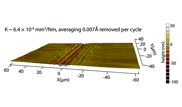
A profilometric scan shows the wear scar left on a GaN coating by a custom microtribometer. The Lehigh researchers found that GaN’s wear resistance exceeds that of sapphire and approaches the wear resistance of diamonds. (Image courtesy of Guosong Zeng) |
“The first time we observed the ultralow wear rate of GaN was in winter,” said Zeng. “These results could not be replicated in summer, when the material’s wear rate increased by two orders of magnitude.”
To determine how the higher summer humidity was affecting GaN’s wear performance, the researchers put their tribometer in a glove box that can be backfilled with either nitrogen or humid air.
“We observed that as we increased the humidity inside the glove box, we also increased the wear rate of GaN,” said Zeng.
Zeng gave a presentation about the Lehigh project earlier this month at the International Workshop on Nitride Semiconductors (IWN 2016) in Orlando, Florida. The session at which he spoke was titled “Wear of Nitride Materials and Properties of GaN-based Structures.” Zeng was one of seven presenters at the session and the only one to discuss the wear properties of GaN and other III-Nitride materials.
Tansu, who has studied GaN for more than a decade, and Krick, a tribology expert, became curious about GaN’s wear performance several years ago when they discussed their research projects after a Lehigh faculty meeting.
“Nelson asked me if anyone had ever investigated the friction and wear properties of gallium nitride,” said Krick, “and I said I didn’t know. We checked later and found a wide-open field.”
Tansu said the group’s discovery of GaN’s hardness and wear performance could have a dramatic effect on the electronic and digital device industries. In a device such as a smartphone, he said, the electronic components are housed underneath a protective coating of glass or sapphire. This poses potential compatibility problems, which could be avoided by using GaN.
“The wear resistance of GaN,” said Tansu, “gives us the opportunity to replace the multiple layers in a typical semiconductor device with one layer made of a material that has excellent optical and electrical properties and is wear-resistant as well.
“Using GaN, you can build an entire device in one platform without multiple layers of technologies. You can integrate electronics, light sensors and light emitters and still have a mechanically robust device. This will open up a new paradigm for designing devices. And because GaN can be made very thin and still strong, it will accelerate the move to flexible electronics.”
In addition to its unexpectedly good wear performance, said Zeng, GaN also has a favorable radiation hardness, which is an important property for the solar cells that power space vehicles. In outer space, these solar cells encounter large quantities of very fine cosmic dust, along with x-rays and gamma rays, and thus require a wear-resistant coating, which in turn needs to be compatible with the cell’s electronic circuitry. GaN provides the necessary hardness without introducing compatibility issues with the circuitry.
The Lehigh group has begun collaborating with Bruce E. Koel, a surface chemistry expert and professor of chemical and biological engineering at Princeton University, to gain a better understanding of the interaction of GaN and water under contact. Koel was formerly a chemistry professor and vice president for research and graduate studies at Lehigh.
To determine the evolution of wear with GaN, the group has subjected GaN to stresses by running slide tests in which the slide distance and the corresponding number of cycles are varied. The group then uses an x-ray photoelectron spectrometer (XPS), which can identify the elemental composition of the first 12 nanometers of a surface, to scan the unworn surface of the GaN, the scar created by the slide machine, and the wear particles deposited by the slide machine on either side of the scar.
The group plans next to use aberration-corrected transmission electron microscopy to examine the lattice of atoms beneath the scar. Meanwhile, they will simulate a test in which the lattice is strained with water in order to observe the variations caused by deforming energy.
“This is a very new experiment,” said Zeng. “It will enable us to see dynamic surface chemistry by watching the chemical reaction that results when you apply shear, tensile or compressive pressure to the surface of GaN.”
Story by Kurt Pfitzer


