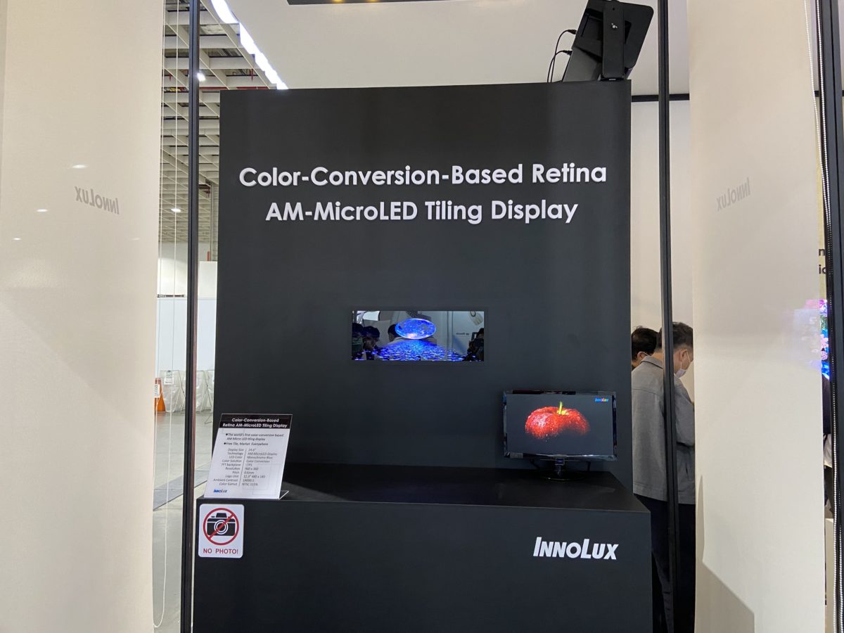
Micro LEDs as a light source has been an advanced technology under the spotlight in the display industry. Numerous Micro LED products were unveiled in the Touch Taiwan exhibition this year. Specifically, AUO, Innolux, and PlayNitride all presented their Micro LED development results, demonstrating the companies’ strategies of strengthening upstream–downstream alliances as well as their determination to overcome the existing technical challenges.

As a promising display approach, the Micro LED technology not only creates better visual experiences but boasts better integration capabilities and performance than its LCD and OLED counterparts. Applications of this advanced technology include AR/VR, wearables, notebooks/car dashboards, mobile devices (e.g., smartphones and tablets), and large-size monitors (e.g., video walls and TVs).
“For the consumer good market, Micro LEDs are still at the R&D and low-volume trial production stages, and most of them are applied to electronic products. It may take two to three years for the technology to be mature enough to be put in high-accuracy products like wearables and smartphones,” said Chan-Pin Chong during an interview with TechNews, who serves as an executive VP for Kulicke & Soffa (K&S), an international manufacturer of semiconductors and advanced display devices. “Although the supply chain R&D and manufacturing has slowed down due to the pandemic, investors are optimistic and have invested in each stage of Mini LED production. They have also directed their investment and partnerships to technology-related aspects.”
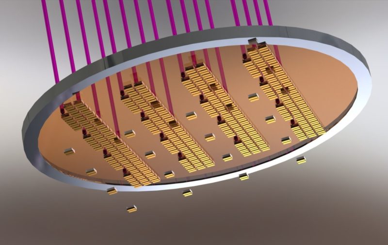
To achieve mass production of Micro LEDs, the mass transfer technology will be a key factor. Currently, stamping process based on the pick-and-place concept is the dominant method for mass transfer. Simply put, pick-and-place stamping involves the use of static electricity, Van der Waals forces, and magnetic force to pick up a large amount of Micro LED chips and move the chips to a target backplane. Several Micro LED manufacturers adopt such mass transfer technology.
The stamping process based on pick-and-place is sufficiently mature for mass production. Meanwhile, the industry has never stopped developing other mass transfer options with the hope of achieving faster, more efficient, and more flexible transfer, among which include laser transfer.
As its name suggests, laser transfer refers to the process of using laser beams to quickly transfer a great number of Micro LEDs from the original substrate to the target one. In this process, a transparent substrate (mostly a quartz or sapphire substrate) is used to carry the components in question through a specific intermediate material. Later, lasers are used to illuminate the transparent substrate and prompt it to react with the intermediate material, whereby selective transfer of components can be realized using photomasks. Depending on the laser wavelength and material property, laser transfer can be further divided into laser direct release and laser ablative release. Leading suppliers adopting the laser transfer process include Uniqarta (acquired by K&S) and QMAT.
Cost Reduction Is the Key for Mass Production of Micro LEDs
Cost reduction has remained the largest challenge for Micro LED displays, of which the production requires processing an immense amount of dies, suggesting that the manufacturing of such components can hardly be cost-effective if the existing technologies and equipment are adopted. The executive VP of K&S Chan-Pin Chong specified that the cost decides whether mass production and commercialization of Micro LEDs are feasible. For example, a 65-inch Micro LED 4K TV currently is priced at no less than US$100,000; to be honest, no consumers can afford placing such a luxury in their living room.
Increasing Yield Rate and Efficiency Are Two Keys to Cost Reduction for Large-Size Micro LED Displays
“The Micro LED technology has yet to mature; especially, we still have a long way to go for cost reduction,” Chong said. “The transfer and repair costs of Micro LEDs are very high, particularly that for single die. If a Micro LED monitor has one or two defective dies which cannot be fixed, the product must be disposed of. To achieve high-accuracy display, those small dies must be transferred to a big screen, which requires a different approach.”
Therefore, suppliers are now endeavoring to modify production equipment, innovate inspection methods, and develop new mass transfer techniques. Since 2018 where it introduced advanced technologies to Mini/Micro LED mass transfer, K&S launched its first-generation mass transfer equipment that pushes the transfer rate to the next level with a unique placement approach.
Chong emphasized that cost reduction is the key to mass production and commercialization of Micro LEDs. Businesses should then focus on manufacturing technologies, among which mass transfer is critical. Presently, Micro LED manufacturers adopt different mass transfer techniques and there is no standard for such process. After studying various mass transfer techniques, K&S decided to adopt laser transfer because the approach can potentially have greater efficiency.
K&S Acquires Uniqarta to Advance Laser Transfer Technology
To advance laser transfer, as revealed by Chong, K&S announced its plan to acquire a US-based tech company Uniqarta at the beginning of this year. The acquisition comprised Uniqarta’s intellectual property rights and patent portfolios. Beforehand, K&S and Uniqarta had established comprehensive partnerships, during which the tech company’s know-how of LED die transfer was commercialized.
Reportedly, Uniqarta’s Laser-Enabled Advanced Placement (LEAP) technology overcomes the existing difficulties of conventional pick and placement by adopting a highly accurate, ultrafast laser transfer placement system. Because of its non-contact nature, LEAP allows die placement in large quantities with an increased transfer rate as well as inspires K&S to develop next-generation high-accuracy solutions, thereby promoting wide application of multi-functional and low-cost display technologies. LEAP, as a cutting-edge LED transfer technology, is expected to speed up the introduction of Mini LED backlights to the market and facilitate the application of Micro LEDs to direct-lit displays.
The VP and CTO at K&S Bob Chylak said that the Uniqarta acquisition has strengthened and expanded K&S’ overall tech portfolios for Mini/Micro LEDs. The acquisition marks an important strategic supplement of team competences and value proposition, enabling the two to comprehensively engage in the booming advanced display market.
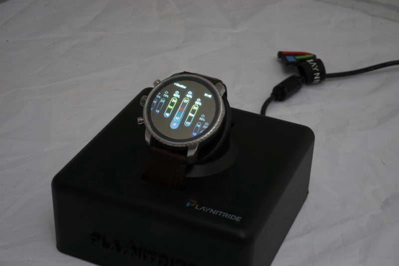
Micro LEDs Will Be First Introduced to Markets of Large Billboards and Wearables
Concerning Micro LED development in the near future, because reducing the production cost is still difficult in the short run, Chong maintains that large-size fine-pitch display products and wearables are two potential applications for Micro LED commercialization.
Products such as billboards and advertising screens do not require extremely high resolution, hence a lower technical threshold of mass transfer. On the other hand, the yield rate of Micro LED epitaxial wafer dicing tends to be better for wearables thanks to their small size, indicating a lower probability of production scrap and thus a lower cost. Accordingly, Chong suggested that in the next few years, the application of Micro LEDs may first focus on billboards and wearables and—until the technology becomes mature—shift to other consumer electronics, such as smartphones, tablets, and TVs.
Chong also disclosed that in addition to actively developing Micro LED technologies, K&S optimizes its facilities per the target LED products. For instance, the company developed ConnX ELITE™ Opto, an LED wire bonding system with the following features: software suite allowing bonding wires of different materials (i.e., gold, silver, copper, and alloy), sensor positioning during wire bonding, built-in magazines and pusher arms, as well as light sources including straight light, edge light, low-angle edge light, and red and blue lights. The machine has functions designed for LED wire bonding.
In sum, ConnX ELITE™ Opto can be optimized as per requirements of the LED product in question, whereby the hardware and process can be improved for optimal output. The equipment also supports wider, thinner lead frames and substrates and allows multiple LEDs—whether or not they are of the same types—to be placed within the same module, thereby facilitating fast introduction and cutting time to market.
(This article is reposted by TechNews, Source of first image: Samsung)


