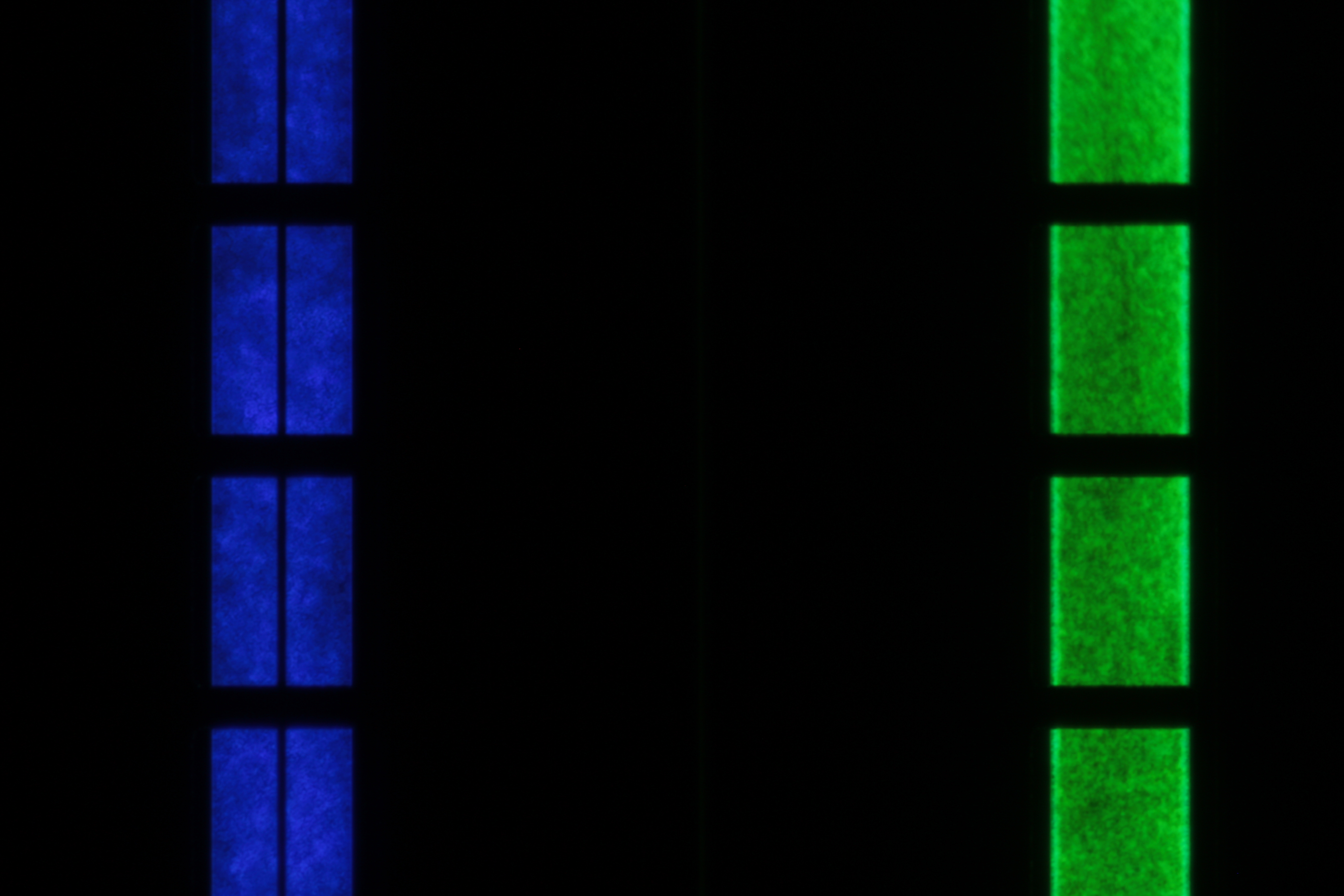
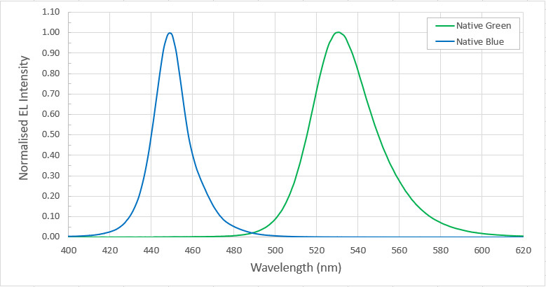
Plessey announced that it has successfully achieved native blue and green color emission on the same epitaxy wafer with its GaN-on-Silicon process.

(Image: Plessey)
To form RGB Micro LED displays, typical approaches are to use a pick and place process to transfer discrete R, G and B pixels or to use Native Blue LEDs as the light source for subsequent color conversion, to Red and Green. But the tiny chip size makes the placement process and conversion very difficult.
Plessey’s latest patented growth approach simplifies the color conversion process by creating both blue and green emission layers on the same wafer. Green Micro LEDs have high efficiency with a narrow spectral width resulting in an excellent color gamut when operating alongside the high performance blue Micro LEDs.
Among the issues preventing the integration of multiple wavelength diode junctions are, firstly, a magnesium memory effect and diffusion from the p-type cladding of the lower junction into the upper junction. An additional process challenge to the integration of Blue and Green Micro LEDs is the precise tuning of the thermal budget during the growth of the second junction to prevent indium phase separation in the blue active region. Plessey has precisely engineered the thermal budget to maintain high efficiency (IQE), low defectivity and high electrical conductivity required for high brightness display applications.
A final operation in the formation of GaN Micro LEDs is a post growth treatment aimed at removing hydrogen atoms that would otherwise compromise the conductivity of p-type layers. The presence of a second junction complicates the removal of hydrogen from the buried device structure negating the effect of standard post-growth activation treatments. Plessey created a monolithic blue and green Micro LED fabrication process that integrates these junctions vertically separated by a sub-micron layer thickness.

(Image: Plessey)


 CN
TW
EN


