Competition in glass substrate-based advanced packaging is intensifying across the semiconductor industry. According to Central News Agency, China is accelerating investment in glass substrate-based advanced packaging, while Taiwan is stepping up efforts to strengthen its competitiveness by integrating its semiconductor, optoelectronics, and equipment manufacturing capabilities.
Intel and China’s Lens Technology announced a strategic collaboration to advance glass substrate-based semiconductor packaging. Institutional investors cited by the report say the partnership will focus on glass core substrate-based advanced packaging, with mass production potentially beginning as early as the second half of 2027.
The report also notes that BOE is expanding into glass substrates and glass core substrate-based advanced packaging. After investing in a pilot production line in 2024 and deploying a fully automated line in the first half of 2026, BOE is developing end-to-end process solutions with chip design customers in China and North America. Institutional investors cited by the report expect mass production to begin as early as 2028.
Taiwan Strengthens Its Advanced Packaging Ecosystem
Meanwhile, Taiwan is also expanding its glass substrate advanced packaging ecosystem, according to Central News Agency. Innolux and AUO are developing fan-out panel-level packaging (FOPLP) using square glass substrates, while Innolux is also advancing glass through-via (TGV) technology. In addition, TPK-KY has invested in a pilot production line for TGV-based glass substrates for advanced packaging at its Taiwan facilities.
OSAT provider Powertech is also expanding its FOPLP capabilities. According to TechNews, during its 2Q26 earnings call, the company said it had officially joined AMD’s AI chip supply chain and aims to become the world’s first OSAT to mass-produce fan-out panel-level packaging (FOPLP) for AI applications by mid-2027. Powertech and Broadcom also previously announced a joint venture in Singapore to develop additive fine-line redistribution layer (RDL) technology for advanced packaging substrates.
Taiwan’s Glass Substrate Opportunity
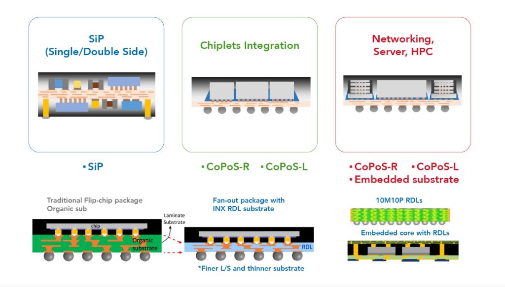
According to TrendForce, fan-out panel-level packaging (FOPLP) is emerging as a new battleground across the semiconductor industry. TSMC is focusing on its Chip-on-Panel-on-Substrate (CoPoS), standardized on a 310 × 310 mm panel format. TrendForce expects 2026 to be a key validation year for equipment and materials suppliers, followed by pilot production in 2027 and mass production in the second half of 2028. Beyond CoPoS, TSMC is expected to shift its next major focus to glass core substrates, with commercial-scale production likely after 2030.
TrendForce concludes that Taiwan’s expertise in large-format glass processing, combined with the advanced packaging and process integration capabilities of its leading semiconductor companies, provides a unique competitive advantage. Supported by a growing ecosystem of local materials and equipment suppliers and aligned with TSMC’s localization efforts, Taiwan is well positioned to shorten the learning curve for glass core substrates and create a new growth path for its panel industry.
(Photo credit: Innolux)


