Japanese technology has always been under the global spotlight and recognized as a worldwide trend indicator. LEDinside observed flip chip LED and EMC will become the major development trend this year among manufacturers display and release of related equipment and material at Lighting Japan 2014, which took place at Tokyo Big Sight earlier this month. Below is LEDinside observations and trend analysis while interviewing equipment, material, and package manufacturers at the trade show:
Flip chip LED technology becomes LED industry new pet
As flip chip LED technology becomes more mature, flip chip products advantages of wire-bonding free and driven by high current meet the end market’s Cost/Performance (C/P) demands. Flip chip LED has become a major development focus for LED manufacturers in 2014.
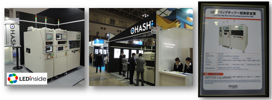
OHASHI has launched LMS-2000 flip chip COB equipment, which is a fully automatic LED flip chip one-shot bonder. The machine handles the four processes of adhesive dispensing, LED flip chip mounting, pre-heating, and one-shot bonding through a single system to provide high accuracy and productivity. Since flip chip technology is becoming more mature, increasing number of manufacturers want to make COB products to leverage flip chip strengths of wire-bonding free and driven by high currents. In general, it is believed the flip chip market will rise in the near future.
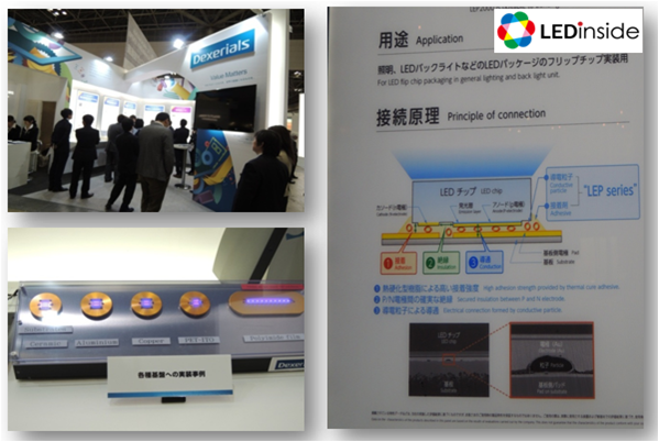
Related materials have also been launched. Dexerials displayed anisotropic conductive adhesive LEP Series (LEP 2000/LEP 3000), the ACF sizes are smaller than 5 um. By using anisotropic conductive adhesive to forcefully connect the substrate, the P-type and N-type can become fully insulated. In the last stage, the ACF finally breaks to complete electric conductivity.
Current AU/SN die bonding must operate at temperatures above 300 degrees Celsius, and can only use ceramic substrates. However by using LEP conductive adhesive, the operation temperature can be lowered to below 180 degrees Celsius. Substrate options are also expanded to glass and PET substrates. Overall, costs in chips, substrate and equipment can be reduced. It is estimated overall costs can be cut by 30 percent compared to AU/SN die bonding. LED manufacturers will only need to acquire thermocompressor with LEP anisotropic conductive adhesive.
 |
|
Dexerial demonstrates anisotropic conductive adhesive LEP Series, which will be applied in flip chip market. |
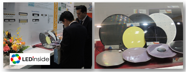
Flip chip LED wafer level packaging has also received market attention. Apic Yamada had established WLP molding systems since 1997. Now, the company has integrated its know-how and technological expertise into the world’s first fully automated WLP molding system released on the market, the WCM-300L. The machine adopts in-line concept to process wafer loading or unloading, compound feeding, encapsulation and visual inspection. The system handles the wafer without any damage nor contamination and encapsulates high quality products. The press system is a high precision mechanical press, specially developed for WLP. This system can handle either liquid or granular compound to accommodate to the customer’s requirement. The WLP technology development can also greatly reduce LED packaging costs.
Currently, there are two kinds of molding processes for wafer level package. First is the Transfer Molding Process, the other is Compression Molding Process with powder type or liquid type. However, transfer molding for WLP is limited to 6 inch wafers, because of compound flow limitation. Compression molding is currently the main stream method. Therefore, Apic Yamada adopts Compression Molding Process to complete the process on reflector, phosphor and lens. Nowadays, Apic Yamada can develop 300mm wafer level package and 340mm squared large panel package. In the future, Apic Yamada plans to release 500x600mm large sized molding technology. The WCM-300L which is originally applied in memory and MEMS fields, is now being released by Apic Yamada to serve the LED market in response to emerging WLP concept in the LED industry.
LED package products introduce EMC lead frame to meet C/P advantages
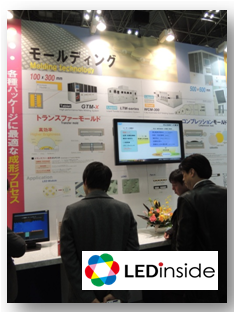
Apic Yamada released EMC lead frame molding machine, which greatly reduces labor costs by using automated production advantages. Observations of EMC lead frame production advantages can be shown by calculating on an hourly production basis of 80,000 pcs, which brings monthly production for 3030 LED lead frames to about 40KK.
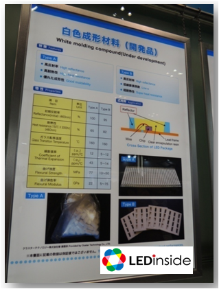
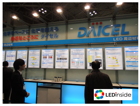
At the moment Hitachi is the exclusive supplier on the market for white epoxy materials for LED lead frames. Since EMC products can endure higher voltage and is cheaper than ceramic substrate, DAICEL is also developing white epoxy material, which is estimated to be released on the market in 2Q14. In addition, at Lighting Japan 2014 the company also displayed molding products co-developed with clients.
Continual material improvements for high temperature, high voltage, and high CRI backlight applications
DAICEL released LED package glue CELVENUS W0970 series and W0930 for LED display products and the CELVENUS W0925(W0926) for display and LED backlight market. Under high temperature and high current tests, CELVENUS product series still maintained good performance after 1,000 hours. This can solve the issue of lead frame vulcanization and diode erosion from using silicon package glue. The company also released its silicon package glue product T-series, which uses DAICEL patented technology. Compared to silicon glue sold on the market, the T-series has the features of vulcanization-resistant and provides excellent thermal resistance.
 |
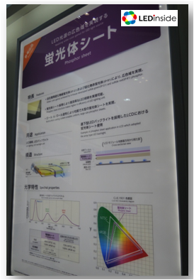
Dexerials also promoted at the show phosphor sheet products, since TV manufacturers are actively introducing 4K2K TV. High quality phosphor is especially popular among LED package manufacturers. Dexerials makes phosphor sheets from red and green phosphor, and assembled with blue chips can achieve 85 percent NTSC. The material is currently introduced into Sony 65” curved TV. Compared to phosphor coating, the sheet has advantages in uniformity. In comparison to QD film production process, Dexerials products can achieve mass production without creating environmental pollution.
(Author: Joanne Wu, Associate Manager, LED Research Division, LEDinsidehttp:// Translator: Judy Lin, Editor, LEDinside)


