By reducing strain with an InGaN layer on a buried oxide, red-emitting InGaN-based microLEDs are tipped to yield higher efficiencies
While phosphide-based structures lead the way for making most red LEDs, their performance plummets as dimensions decrease. When shrunk below 10 µm, which is the size these microLEDs need to be for displays for virtual and augmented reality, losses are exacerbated by long carrier diffusion lengths and a high density of surface defects at sidewalls.
Pioneering an alternative is a French partnership between the University of Grenoble-Alpes and Soitec. This team is developing red-emitting GaN-based LEDs that suffer from far less strain than equivalents grown on conventional substrates, thanks to deposition of epitaxial layers on an InGaN layer sitting on a buried oxide.
This foundation, formed using Soitec's proprietary Smart Cut process, enables thin InGaN quantum wells to span the entire visible spectrum, thanks to enhanced indium incorporation that results from an increase in the in-plane lattice parameter.
Another benefit of the InGaN platform is that it trims the internal electric field in the device's active region, opening the door to higher efficiencies.
Last year the French team reported the results of red-emitting microLEDs, made on InGaN Smart Cut substrates, that had device dimensions ranging from 300 µm by 300 µm to 50 µm by 50 µm. The latest results, realised with an improved process, are for devices with dimensions down to 10 µm.
Two variants have been used for this latest work: one substrate has a 120 nm-thick InGaN seed layer with an indium content of 8 percent; and the other, identical in thickness, has an 11 percent indium content. Both feature a step meandering substrate morphology and V-shaped defects with a density and size rising with indium content. Upping the indium content increases the density and size of the V-pits from 3 x 107 cm-2 and 100 nm to 2 x 108 cm-2 and 130 nm.
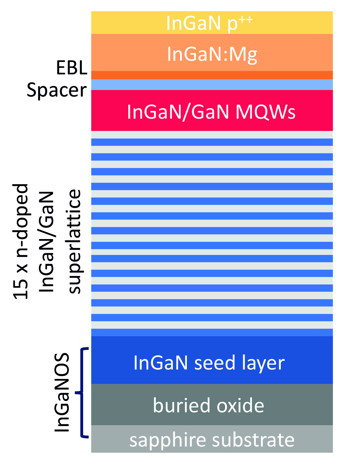
Device fabrication began by loading substrates into an MOCVD reactor and depositing an epitaxial stack that included a 15 period superlattice, a multi-quantum-well active region and an electron-blocking layer . The picture above shows the details of the superlattice with n-type In0.03Ga0.97N/GaN layers provided a foundation for the active region, containing five 2 nm-thick In0.4Ga0.6N quantum wells, separated by 7.5 nm-thick In0.03Ga0.97N barriers. The 15 nm-thick electron-blocking layer is made from Al0.1Ga0.9N.
Scrutinising this heterostructure with a high-resolution transmission electron microscope revealed additional dislocations in the active region and electron-blocking layer, attributed to local strain relaxation.
The team employed conventional LED chip fabrication processes to fabricate LEDs with mesa sizes ranging from 300 µm by 300 µm to 10 µm by 10 µm. The previous portfolio of devices were held back by V-shaped defects - when they go through the entire structure, they create an electrical path from anode to cathode. To eradicate this issue, the fabrication process for the latest generation of emitters includes the addition of a conformal layer, planarized with chemical mechanical polishing.
Photoluminescence measurements revealed that the increase in the indium content of the substrate shifted the microLED emission peak from 635 nm to 653 nm. The longer wavelength resulted from a higher a lattice parameter.
For a device with 10 µm-diameter, the maximum external quantum efficiency is 0.14 percent, realised at 8 A cm-2. This value, inferior to that of 0.2 percent by a team from UCSB, is held back by a lower light extraction efficiency. For the device produced by the French team, light is collected from the backside, while the p-contact pad does not cover all of the top of the structure, and no metal prevents light from escaping the sidewalls. Extraction is also hampered by emission that goes through the backside of the device having to traverse the superlattice, buried oxide and sapphire substrate. The actual value for light extraction efficiency is difficult to estimate, but based on simulations, it is below 4 percent.
To improve performance, effort must be directed at increasing the extraction efficiency, trimming the operating voltage, and improving the crystalline quality of the LED.
Reference
A. Dussaigne et al. Appl. Phys. Express 14 092011 (2021)


