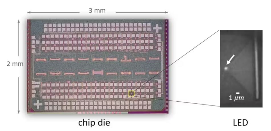
Smaller than the wavelength of light it emits, this tiny silicon LED could mean a big breakthrough for microscopy and more.

A research team from the Singapore-MIT Alliance for Research and Technology (SMART) claim to have built the "world's smallest LED" — and say the technology could be used to turn smartphone cameras into high-resolution microscopes in the future.
"Our breakthrough represents a proof of concept that could be hugely impactful for numerous applications requiring the use of micro-LEDs," claims Iksung Kang, research assistant at the Massachusetts Institute of Technology at the time of the project and lead author of the paper detailing the work. "For instance, this LED could be combined into an array for higher levels of illumination needed for larger-scale applications."

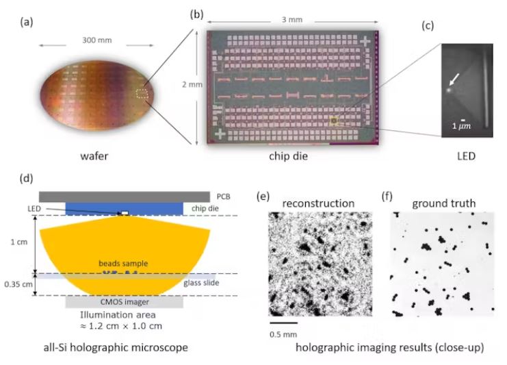
The world's smallest LED(a.b.c), with some machine-learning smart, could turn future smartphones into microscopes (d,e,f).
"In addition," Kang continues, "due to the low cost and scalability of microelectronics CMOS processes, this can be done without increasing the system’s complexity, cost, or form factor. This enables us to convert, with relative ease, a mobile phone camera into a holographic microscope. Furthermore, control electronics and even the imager could be integrated into the same chip by exploiting the available electronics in the process, thus creating an 'all-in-one' micro-LED that could be transformative for the field."
The silicon LED created by the team is definitely tiny — smaller even, interestingly, than the wavelength of the light it emits. Despite this, its light intensity is equivalent to much larger silicon LEDs — and it's powerful enough to drive a prototype holographic microscope, which forms the base of the team's claims to be able to convert smartphone cameras into microscopes through integration of the LEDs at a silicon level.
To actually make the microscope — stand-alone or built into a smartphone — work, though, requires some clever software. In this case, that software is a deep neural network algorithm which is able to turn measurements made by what the team calls a "holographic microscope" into reconstructed objects. In testing, the hardware and software combo proved capable of peering at objects as small as cells and bacteria without bulky optics.

Using the tiny LEDs and a neural network, the team has created tiny "holographic microscopes."
"On top of its immense potential in lensless holography, our new LED has a wide range of other possible applications," claims co-author Rajeev Ram, professor of electrical engineering at MIT and co-author.
"Because its wavelength is within the minimum absorption window of biological tissues, together with its high intensity and nanoscale emission area, our LED could be ideal for bio-imaging and bio-sensing applications, including near-field microscopy and implantable CMOS devices. Also, it is possible to integrate this LED with on-chip photodetectors, and it could then find further applications in on-chip communication, NIR [Near Infrared] proximity sensing, and on-wafer testing of photonics."
The team's paper on the silicon LED has been published in the journal Nature Communications, while the deep neural network for holographic microscopy is described in a paper published in Optica — both under open-access terms.
TrendForce 2022 Micro LED Self-Emissive Display Trends and Analysis on Supplier's Strategies
Release date: 31 May 2022 / 30 November 2022
Format: PDF
Languages: Tradional Chinese / English
Pages : 130–150 in total (subject to change)
|
If you would like to know more details , please contact:
|


