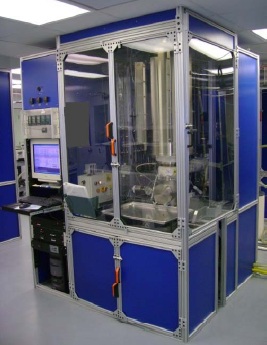
Kyma Technologies has tapped into the market for GaN crystal growth equipment.
The firm’s GaN crystal growth system is based on the hydride vapour phase epitaxy (HVPE) growth process which is a proven high growth rate approach for producing high purity crystalline compound semiconductor materials including GaN, GaAs, InP, and CdS.
HVPE is the dominant process used today for production of free-standing GaN substrates and recently has been used by Kyma and others to produce high quality GaN on sapphire templates and GaN on silicon templates. HVPE grown GaN templates have major advantages over free-standing GaN in terms of cost per unit area and diameter scalability.
The market for nitride semiconductor devices was around $9 billion in 2011 and is expected to surpass $60B over the long term, including $30B in visible lighting applications and $30B in power electonics applications.

Kyma100 HVPE system
Introduction about Kyma’s new product
Kyma’s new product offering is called the Kyma100 HVPE System and leverages over a decade of company experience in the design, construction, and application of HVPE process equipment for manufacturing GaN materials. It’s high purity, vertical flow, hot wall design supports production of n-type conductive GaN at growth rates up to 500 µm per hour. The background impurity concentration is less than 1x1017cm‐3. Complete with a process for production of high quality GaN on sapphire templates, the system can grow up to three 2-inch diameter wafers or one 4-inch diameter wafer at a time.
“Demand for our AlN and GaN template products is growing, yet many of our volume customers prefer to bring the template manufacturing process in-house,” says Keith Evans, Kyma president & CEO. “Adding HVPE equipment to our product line is a natural step in Kyma’s growth, and represents the first of several new equipment product offerings we plan to announce in the coming weeks.”


