Traditionally Gallium Nitride (GaN) LED devices are produced on either sapphire or silicon carbide (SiC) substrates, due to the good crystal lattice matching between the materials and the GaN, with typically 2” or 4” diameter material being used. Significant effort is being made to grow GaN on ubiquitous larger diameter (6” or greater) silicon wafers, a substrate that offers significant substrate cost reduction, together with the ability to process in automated IC production lines. Reasonable estimates are that potential savings on the order of 80% over traditional production methods will result.
The issue with silicon, however, is that it is mismatched severely both mechanically and thermally from GaN, which can result in severely bowed wafer growth and poor quality crystalline material from which to construct an LED device. Today’s GaN on silicon technology, acquired through Cambridge University spin out CamGan in 2012, resolves these mismatch issues and has successfully transferred to its fabrication facility in Plymouth, UK. As a result, the first commercial GaN on silicon low-cost, entry level LEDs are now hitting the market. These initial products, aimed at the indicator and accent lighting market have efficacy levels of 30-40 lumens per watts, with higher level products above 70 lumens per watt expected in Q3 and Q4 of this year for the more general lighting market.
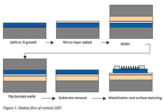
Utilizing silicon substrates in the production of an LED requires a number of process steps to overcome the inherent silicon light absorption in the structure and to enable an efficient device to be produced. In the fabrication process, illustrated in Fig.1, a vertical LED device is designed from a GaN structure grown by MOCVD on a 6” silicon wafer. A highly reflective (typically 95% reflectance) contact is deposited and annealed, followed by several further metallization layers intended to adhere the wafer to a surrogate substrate.

Bonding is then performed, using electrically and thermally conducting eutectic Au-Sn layer, giving a re-melt point of ~280°C, with extra metal layers to act as a barrier between the bonding metals and the device or surrogate when the bonding layers are molten. After bonding, the parent wafer is removed to expose the seeding layer used in the epitaxial growth of the GaN layers. The flipped wafer is aligned to allow subsequent processing of patterned LED devices. Metal tracks are patterned on top of the wafers that lie over a blocking layer to minimize the amount of emitting area covered. Most of the current is intended to be carried by the top metal, typically 2mm. Finally, patterning for light extraction is performed, etching down into the GaN layers exposed post bonding and parent wafer removal. This last step is particularly critical for remote phosphor application as it allows the control of the emission pattern of the blue emitting LED.
Since the refractive index of GaN semiconductor is high (approximately 2.45 at 455nm – blue light), only a small fraction of the light generated escapes to the free space. According to Snell’s Law, the narrow escape cone of light in this case is about 25 degrees. If we assume the light generated inside the semiconductor has a uniform spatial distribution and the mirror is greater than 90% reflective, then just 8% of the overall generated light can escape from the top surface of the semiconductor, the remaining being trapped inside by total internal reflections and ultimately absorbed by the constituent materials.
To enhance the light extraction a straightforward design solution consists of coupling the semiconductor to a large dome-like lens with of a radius greater than 1.5 times the size of the emitting area of the semiconductor. Ideally the dome lens should be made of a material of similar refractive index as GaN, n~2.45, which would allow over 90% of light to escape to free space.
In practice, there is no cost-effective material with a refractive index that could match with GaN to make the dome lens and LED manufacturers commonly rely instead on readily available epoxy or silicon-based materials with a typical refractive index of about 1.5. However, adding a dome lens with a refractive index of 1.5 achieves merely 12% light extraction. To overcome the poor performance in light extraction due to total internal reflections it is necessary to modify the light’s optical path to increase the probability to be within the escape cone.
The most conventional and cost-effective method to extract light efficiently is based on surface roughening techniques. This surface technique is also critical because it defines angular emission of the resulting light from the LED device. It is particularly relevant for a remote phosphor application as it allows the control of the emission pattern of the blue LED. Other methods are reported where a patterned reflector is used to scatter light and allow further improvement of light extraction. In nature similar microstructures, such as in firefly lanterns, are found where pattern of jagged scales in the internal structure of firefly are able to enhance the lantern’s glow.
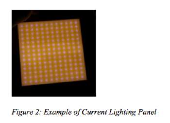
Most LEDs emit light in a spatial pattern where the intensity varies with the cosine of the angle of emergence, providing the standard Lambertian distribution. When these standard LEDs are used in an array to form lighting panels, the resulting light spread is a pattern of undesired singular light emission points, as illustrated in fig. 2, often referred to as “hot spots”. In fig. 2, the LED intensity is kept low to help illustrate the problem.

In order to extract light and generate a far more uniform light pattern, which provides a more aesthetically pleasing result to the consumer, the LED light extraction should be designed to emit in a non-Lambertian distribution, typically batwing. This will have the effect of extending the light illumination over a wider lateral area, thereby maximizing the phosphor pumping efficiency and reducing losses through improved blue light conversion. The consequence of achieving this goal is that the LEDs comprising such a light panel can be spaced more widely, ultimately reducing the overall production costs of the resulting luminaire system.
The overall energy savings through this light path extraction engineering is estimated to be 10%, with subsequent assembly cost savings if the number of LEDs required is reduced. The reduction will be dependent on the level of light intensity patterning achieved. A 50% reduction in LEDs could be achieved with a good batwing type distribution while maintaining or improving on the intensity variations in the phosphor. The light path design is to be implemented through careful surface patterning and imprinting techniques and will utilise computer simulations to optimize both the spatial distribution and the light extraction.
By combining low cost GaN on silicon base technology together with light extraction engineering from the LED design, it becomes possible to design cost-effective glare-free luminaires by using optimized configurations of low power LED arrays.
‘Smart Lighting’ will continue to take LED technology beyond simple energy saving and into systems that encompass sensors and user interface capabilities. Examples are ambient light monitoring for even greater energy efficient usage, user detection and even the potential for light communications, where the high switching capabilities of LEDs are exploited to transmit data.


