Oji Holdings Corporation has established the fabrication technology of patterned sapphire substrates (PSS) for LEDs which improves the performance of front luminance of LEDs by more than double compared to that of LEDs with non-structured sapphire substrate, by applying the technique of precise coating with fine particles.
1. Features of Newly Developed PSS
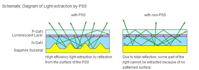
Technologies which can enhance the light extraction efficiency of LEDs by applying sapphire substrate with fine structure are widely used in LEDs. Sapphire substrate of these kinds is called the “PSS” (Patterned Sapphire Substrate).
Schematic Diagram of Light-extraction by PSS

Oji Holdings Corporation has developed the technology of mass production for the PSS by applying the technique of precise coating with fine particles. Delivery of customer sample of this PSS is planned to start in the near term. Pattern pitch of the PSS fabricated by this newly developed technology can be extensively controlled in the range from approx. 3um as maximum (1um = thousandth part of 1mm) to approx. 200nm as minimum (1nm = millionth part of 1mm; PSS with 200nm-pitch pattern is difficult to be fabricated by using mature technique at this moment). Also, by this new technology, PSS can be formed in various shapes as circular cone, bell, and dome as well as various sizes. Moreover, this technology made it capable to produce 6 inches diameter wafers which is the maximum size for the production line of LEDs.
Improvements of LEDs using the newly developed PSS have been confirmed as below:
i) Front luminance (at a wavelength of 385nm):
2.4 times higher luminance than that of the flat sapphire substrate, and 20% higher luminance than that of conventional PSS
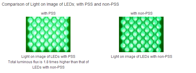
ii) Total luminous flux (at a wavelength of 385nm):
1.8 times higher than that of flat sapphire substrate

The optimum structure of the PSS is dependent on the layer structure of LEDs and the light wavelength of the emission. The newly developed PSS have high controllability of the pattern pitch and the shape of the PSS. This flexibility of the PSS made it possible to create fine and optimum shapes.
(Fig.1 and Fig.2 show secondary election imges of newly developed with sub-micron pitchPSS.)

Furthermore, newly developed technology can provide a “combination structure”. The combination structure consists of the pattern with several hundred nanometer pitch which is considered to improve the quality of deposition during fabrication process of LEDs, and the pattern with several micrometer pitch which is effective to improve the light extraction from LEDs.
(Fig. 3 and Fig. 4 show secondary electron images of the PSS examples with combination structure.)

The combination structure enhances efficiency of the light-extraction of LEDs. As described above, the newly developed PSS by applying the simplified technique of the precise coating must be useful to achieve the further enhancement of the luminance of LEDs.


