Most modern electronics, from flat-screen TVs and smartphones to wearable technologies and computer monitors, use tiny light-emitting diodes, or LEDs. These LEDs are based off of semiconductors that emit light with the movement of electrons. As devices get smaller and faster, there is more demand for such semiconductors that are tinier, stronger and more energy efficient.
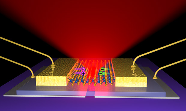
University of Washington (UW) scientists have built the thinnest-known LED that can be used as a source of light energy in electronics. The LED is based off of two-dimensional, flexible semiconductors, making it possible to stack or use in much smaller and more diverse applications than current technology allows.
 |
|
This graphical representation shows the layers of the 2-D LED and how it emits light. (Image Courtesy of University of Washington) |
“We are able to make the thinnest-possible LEDs, only three atoms thick yet mechanically strong. Such thin and foldable LEDs are critical for future portable and integrated electronic devices,” said Xiaodong Xu, a UW assistant professor in materials science and engineering and in physics.
Xu along with Jason Ross, a UW materials science and engineering graduate student, co-authored a paper about this technology that appeared online March 9 in Nature Nanotechnology.
Most consumer electronics use three-dimensional LEDs, but these are 10 to 20 times thicker than the LEDs being developed by the UW.
“These are 10,000 times smaller than the thickness of a human hair, yet the light they emit can be seen by standard measurement equipment,” Ross said. “This is a huge leap of miniaturization of technology, and because it’s a semiconductor, you can do almost everything with it that is possible with existing, three-dimensional silicon technologies,” Ross said.
The UW’s LED is made from flat sheets of the molecular semiconductor known as tungsten diselenide, a member of a group of two-dimensional materials that have been recently identified as the thinnest-known semiconductors. Researchers use regular adhesive tape to extract a single sheet of this material from thick, layered pieces in a method inspired by the 2010 Nobel Prize in Physics awarded to the University of Manchester for isolating one-atom-thick flakes of carbon, called graphene, from a piece of graphite.
In this video, UW researchers demonstrate a technique to isolate a single layer of the material graphene. This simple technique, commonly used by scientists worldwide, can isolate monolayers of many materials.
In addition to light-emitting applications, this technology could open doors for using light as interconnects to run nano-scale computer chips instead of standard devices that operate off the movement of electrons, or electricity. The latter process creates a lot of heat and wastes power, whereas sending light through a chip to achieve the same purpose would be highly efficient.
“A promising solution is to replace the electrical interconnect with optical ones, which will maintain the high bandwidth but consume less energy,” Xu said. “Our work makes it possible to make highly integrated and energy-efficient devices in areas such as lighting, optical communication and nano lasers.”
 |
|
A close-up view of a single layer of atoms of the semiconductor material, tungsten diselenide, on silicon oxide. The ability to see the contrast of the single layer of atoms against the background shows how strongly these materials interact with light. (Image Courtesy of University of Washington) |
The research team is working on more efficient ways to create these thin LEDs and looking at what happens when two-dimensional materials are stacked in different ways. Additionally, these materials have been shown to react with polarized light in new ways that no other materials can, and researchers also will continue to pursue those applications.
Co-authors are Aaron Jones and David Cobden of the UW; Philip Klement of Justus Liebig University in Germany; Nirmal Ghimire, Jiaqiang Yan and D.G. Mandrus of the University of Tennessee and Oak Ridge National Laboratory; Takashi Taniguchi, Kenji Watanabe and Kenji Kitamura of the National Institute for Materials Science in Japan; and Wang Yao of the University of Hong Kong.
The research is funded by the U.S. Department of Energy, Office of Science, the Research Grant Council of Hong Kong, the University Grant Council of Hong Kong and the Croucher Foundation. Ross is supported by a National Science Foundation graduate fellowship.


