The Japanese component manufacturing company Namiki recently announced several technological advancements and equipment upgrade for advanced industrial component production. Namiki successfully produced unprecedented large sized diamond substrates and realized the bonding of two different materials under room temperatures; moreover, the corporation reinvented its cleaning system enabling defect-free small scale wafer cleaning and drying.
Large Sized Diamond Substrate
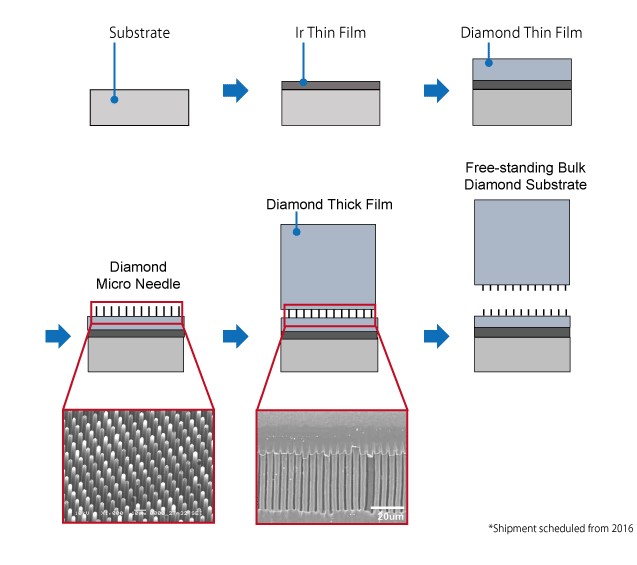
Long known as one of the top industrial jewel parts suppliers, Namiki has been continuing to improve its jewel substrate manufacture technology since 2016 when it mass produced 14mm*14mm single crystal diamond substrates for post-Si semiconductors that build optical parts, heat spreader, audio parts and quantum computer. At present, Namiki is able to manufacture substrates in the size of around 1 inch square with the exclusive, patented microneedle growth technology enabling stable production of crack-free large diamond substrate. Carrying on with the technology, Namiki promised to scale up the size of its substrate products to up to 50mm*50mm (2 inch square) by 2019.
 |
|
Namiki’s newly-developed microneedle growth technology (Image: Namiki)
|
Room Temperature Bonding
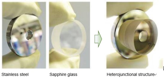
Working temperatures are the linchpin of bonding of two different materials and they hugely affect thermal parameters of those materials bonded. Material bonding, especially metal bonding, is usually conducted under high temperatures, and in some cases under low temperatures. Namiki; however, realized the room temperature bonding of sapphire and metal. With the use of Au sputtering film, it effectively eliminates O-ring and screw fastening in the chamber view ports and creates an ideal structure. Also, the technology can connect two materials with different thermal expansion.
 |
 |
|
The bonding of sapphire and metal under room temperatures using Au sputtering films (Images: Namiki)
|
Advanced Wafer Cleaning System
Cleaning compound semiconductor substrates (SiC, GaN, ALN, sapphire and diamond) for advanced technology is crucial yet not easy. This is because wafer cleaning systems have been developed keeping step with upsizing wafer diameter. Most of the single wafer spin processors now available in the market are intended for 6” or larger sized wafers. Therefore, engineers involved in developing substrates have had to clean them using beakers and tweezers due to lack of appropriate equipment. Namiki developed a unique cleaning system featuring a cleaning brush, mega sonic rinsing and patented drying system especially for small sized substrates.
 |
|
Namiki redeveloped the cleaning system suitable for small scale substrates. (Image: Namiki)
|


