(By George Powch and Ajay Jain)
Why is it Important
Micro-displays in wearables, whether Augmented Reality (AR), Smartwatches, Smartphones or other applications of the near future are not bright enough to readily see images on a bright, sunlit day, nor efficient enough to give mobile devices much loiter time – better technology is needed, particularly as pixel sizes shrink in next gen micro-displays
Micro-display technologies have typically used reflective, transmissive or transreflective architectures relying on color filters with white light or phosphors, increasingly now including Quantum Dot (QD) enhancement, much like larger displays, monitors and TVs, but scaled down. For applications with larger pixels (e.g. >>20 µm), tethered to wall power, where ambient background lighting is not high and lower efficiency tolerable, these have worked reasonably well. Even current mobile devices such as tablets and cellphones still largely use LCD technology, although emissive AMOLED technologies are being rapidly adopted. But all such display technologies are generally difficult to see at high noon on a bright day, and who hasn’t bemoaned a low battery indication on their mobile device?
AMOLED micro-displays are also the default technology for today’s Virtual Reality (VR) applications, whether smartphone based, or any of the Head Mounted Displays (HMDs) coming from HTC Vive, Oculus, Microsoft, and many others … But VR is a markedly different application in presenting a direct view, self-contained world to the observer, where ambient lighting is controlled, and overall display brightness can be low vis-à-vis the dynamic range of the human eye, which can be greater than 106:1!
Indeed, the dark-adapted eye has been shown to detect a single photon, but in display applications, the issue is not absolute sensitivity as much as contrast sensitivity. Against a bright background, the displayed image must be sufficiently bright for contrast or it will melt into the background. For this reason, you can’t see your cellphone screen in the sun at noon on a bright day, and why AR content today is typically demonstrated against dimly lit backgrounds.
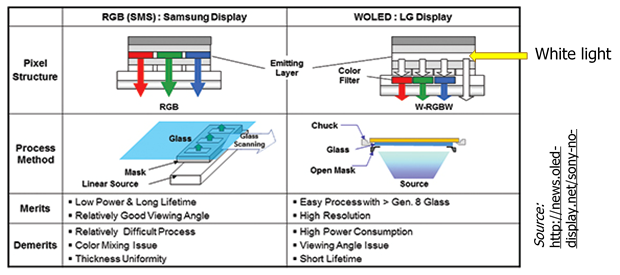
While older technologies such as LCOS or variations of DLP based approaches have been used in AR-type systems, particularly for military, HUDs and professional uses, the current crop of AR systems, especially consumer oriented HMDs all tend to use self-emissive OLED micro-displays at their core, typically, for example, as following leading examples indicate:
The Problems
OLED micro-displays have major issues, however, partly depicted above. They are not nearly bright enough, especially in blue: increasing brightness requires more current and/or larger sized pixels, limiting resolution and/or increasing power consumption (mobile device battery life), while driving blue harder severely curtails already short lifetimes of OLED emitters, with poor color balance. If used to first create white, as is common, then filtered for RGB colors, over 66% of the white light is lost for each color, a very inefficient approach. OLED emitters are also not particularly narrow spectrally, nor at all directional, requiring a backside reflector to emit in at least a half-sphere.
Many of the leading developers of next generationAR systems also proposeto use sophisticated diffractive/ holographic waveguide elements to transfer an image from the location of micro-display (which can be remote) onto the viewer’s field-of-view. The efficiencies of these optical elements tend to be extremely sensitive to the angle and spectra of input light, for which narrow spectral widths and confined cone angles of light from a micro-display will play an increasingly important role.
MicroLED Micro-displays: Wave of the Future
A better, brighter, more efficient display technology with high dynamic range is needed for all these reasons and more. Many players recognize the challenges and have been working on solutions, some quietly, others less so. Some are also exploring Virtual Retinal Displays (VRD) with very low power RGB lasers scanning images directly into the eye. Others (Ostendo) attempt to integrate 3D heterogeneous electroluminescent
LED layers for the different RGB colors, with major manufacturability challenges. But leading among potential solutions may be inorganic microLEDs or the same familiar GaN /InGaN LED technology broadly used in solid state lighting (SSL), but scaled down to microscale sub-pixels (RGB sub-pixels/pixel). Such LED technology brings significant advantages: it is intrinsically some 103 brighter (hence so much more efficient) than OLEDs, and far more environmentally robust, a long lived, fully inorganic structure switching at semiconductor speeds (ns). And importantly, it is well known, accepted core technology … but it also has significant manufacturing challenges.
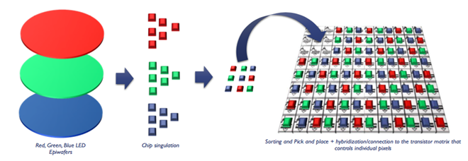
At larger pixel sizes (>50 µm), individual micro-die from separate epitaxial wafers (e.g. R,G,B) can be rapidly assembled using one of several massively parallel approaches, as depicted below:
(Courtesy of Yole Développement )
This is an approach pioneered by LuxVue (acquired by Apple), for example, variations of which pursued by X-celeprint, as well as ITRI, CEA-LETI, SONY and others. The enormous challenge of all these approaches, aside from integrating different material sets, is ensuring 100% placement, since missing a sub-pixel in a small display is unacceptable. Finally, these approaches tend to impracticality when sub-pixel sizes get smaller (<10 µm), limiting range of applications to smartphone or perhaps smartwatch displays, but not AR which may ultimately require sub-pixels << 10 µm.
For next gen VR / AR, micro-displays will evolve toward microLED technology with PPI’s > 1500 and sub-pixel sizes <<10 µm, and with sophisticated optics to transfer the image onto a user’s field-of-view. As pixel sizes shrink <20 µm, the entire micro-display will have to be manufactured at wafer-scale as a monolithic structure, save perhaps for “hybridization” or interconnecting to the Active Matrix CMOS backplane with the switching and control circuitry, a thorny problem in itself as sub-pixel sizes shrink. The evolution of sub-pixel sizes vs. pixel density (PPI) for different applications may be depicted as follows:
(per Yole Développement with permission):
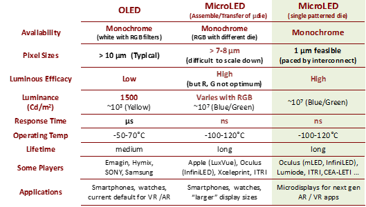
The inherent advantages (and acceptance) of GaN /InGaN-based LED technology has already led to much work to apply it cost effectively to self-emissive displays vis-à-vis OLED displays; it is already used for very large displays: stadium scoreboards, billboards, etc. and has been occasionally sighted at trade shows for TVs (see Sony’s CLEDIS technology). Many are working on scaling microLED technology to micro-displays for broader consumer markets, with manufacturing challenges looming large. A comparative summary of the leading micro-display technologies might look like this, where how you get color is a common issue, since GaN /InGaN-based LED technologies tend to be monochrome (blue/violet) emitters:
Color Conversion Challenges
While far brighter, long lived and efficient than OLEDs, GaN /InGaN-based LEDs are (with some exceptions) monochrome, typically blue/violet emitters, and must be down-converted to Green and Red for multi-color (RGB) or white light. For LEDs in lighting applications, this is typically done with Phosphors. Quantum Dots (QDs) also play an increasing role, both in sharpening the spectral response of traditional phosphors or altogether replacing them in certain applications; however, major issues come into play as pixels shrink <20 µm and even larger, rendering both impractical …
In a micro-display for AR / VR applications, the system level design considerations for color conversion are very distinct from those in a general purpose, direct view, lighting or display application. The practical question is how much of the color converting media is needed above a sub-pixel to ensure enough of the blue/violet pump light is absorbed for good color conversion, since even one bad sub-pixel can render the entire micro-display unusable.
For example, the absorption coefficient for traditional phosphors and nanophosphors (e.g. used for SSL) is some 2-3 orders of magnitude smaller than that for a direct bandgap semiconductor in the visible. This implies that to absorb equivalent input light, a traditional phosphor layer will be some 100x to 1000x thicker than the direct bandgap semiconductor. It becomes quickly apparent that a column at least 100-300 µm thick would be needed above a 10 µm sub-pixel! While an efficient “On-Chip” solution for SSL, the necessary layer thickness, scattering, and inability to pixelate preclude traditional phosphors or nanophosphors as a viable solution for high resolution microLED micro-displays.
Similarly, while semiconductors, a review of existing QD technology indicates they need to be >> 7 µm to absorb most light. More critically, however, most QDs in use today are temperature sensitive and cannot handle high optical flux, so are typically used only in “remote” configurations or where optical flux density is low. However, the optical power density in microLED micro-displays is far greater than in typical SSL applications, potentially >100 W/cm2, far higher than QDs are known to tolerate at present. And questions regarding fine pitch pixelation, uniformity, the practicality and uniformity of dispensing over local vs. global areas, and costs, also remain unanswered.
A potential solution is to use Quantum Wells (QWs) rather than QDs: they are approximate analogs of each other, the QW a 2D version of a monolayer of QDs. Both rely on quantum confinement effects /bandgap engineering to tailor the output wavelength (color), using the thickness of the QW vs. diameter of the QD. While the appeal of QDs is that they can be made inexpensively using liquid colloidal chemistry, the appeal of QWs is that are wholly inorganic semiconductors with better thermal properties, and can be made wafer scale in a vacuum chamber with the better uniformity, consistency, and repeatabilityneeded for micro-display applications.
The same basic system considerationsas with QDs remain, however: you still need sufficient thickness to ensure near full absorption of input light and a method to pixelate the QWs into RGB pixels overlaying the microLED pump array, while preventing inter-pixel crosstalk. Since QWs are continuous 2D films of inorganic semiconductor materials, however, patterning and pixelation can be readily done with existing, conventional technology.
The principal approaches can be summarized as follows:

Finally, there is still another technology for color conversion, a variation to the QW approach for microLED micro-displays with sub-pixels <<10 µm. It gets around the principal challenges, yet may be easiest to implement and scale, while bringing some unique advantages, principally in raw conversion efficiency as well as offering some control over the output spectra and directionality, both of which also enhance system efficiency and color quality.
Branded Chromover™ technology by its creator, VerLASE Technologies (Bridgewater, NJ), it obviates the complex QW stack otherwise needed in the QW approach by integrating a much thinner, simpler QW layer with a novel resonator which lets the input light be near fully absorbed in the thinner QW stack. At the same time, the resonator is designed to also meet output resonance conditions selecting for color /spectral width.
The emission can be in half-sphere, but depending on the application, the resonator can be designed to also confine the output within a narrower cone angle; i.e. the output can be made a highly directional, low étendue source. In the extreme, if the input is a laser, the downconverted output can even be designed to also lase; i.e. as an optically pumped VCSEL, even enabling such arrays in the visible. The structure presents as a monolithic thin film sandwich < 5 µm thick atop a carrier substrate as follows:
A thin film, monolithic chiplet, it is made wafer scale using widely available, conventional processes. For RGB, demo QWs have been made using the same II-VI materials as the best QDs: ZnSe/ZnCdSe/ZnSe, which are well proven, although the resonator technology is materials agnostic and can be designed for III-Vs or any other material set, including for applications in UV or NIR.
Two QW layers are used in a red / green color converting layer married to an underlying blue microLED display, with pixelation accomplished through conventional patterning processes. The structure is engineered for a given micro-display, and there are benefits from close integration with the microLED manufacturing process flow; however, the key Chromover™ layers must be grown separately.
VerLASE’ business model is to work with the microLED manufacturers to customize the color converting layer to their particular requirements. For example, key concerns in all approaches is maximizing the input light into the color converting layer, maximizing extraction efficiency, and mitigating inter-pixel crosstalk. MicroLEDs tend to emit Lambertian (wide angle) light, potentially illuminating adjacent pixels, while efficiency can be enhanced with lower divergence (collimated) pump light, with various schemes being pursued by the microLED developers.
For example, inter-pixel cross talk depends highly on the placement of the color converter layer (proximity to the pump light source), or whether it can be directly bonded to the microLED array. When not directly bonded, there are two potential sources of inter-pixel cross talk noise: (1) where input light strikes the color converter region of an adjacent pixel, thus illuminating it (Out-of-Plane inter-pixel crosstalk), or (2) where down converted light from one lit pixel walks into adjacent pixels (In-Plane inter-pixel crosstalk). In the first case, the resonator architecture has a narrower acceptance angle (e.g. ±15°), preventing pump light at higher angles from being absorbed by adjacent pixels; it is instead waveguided to the edge. In the second case, black masks or pixel definition layers are used to mitigate this type of in-plane pixel cross-talk.
Other Considerations: Directionality and Color
Directionality in emitted output is stressed again, since various specifications tend to ignore its importance, dwelling only on conversion efficiency of the color converter, but the more accurate figure of merit is the net useful light delivered to where it is needed. Most downconverting media emit omnidirectionally, unless some reflecting scheme is used to redirect light, which introduces cost and complexity. Merely concentrating light from an omnidirectional emitter to a solid angle of one Steradian (Ω) represents approximately a 12x improvement; the novel Chromover™ resonator is the only known scheme that can intrinsically concentrate emitted light within approximately such cone angle (although other mechanisms based on how it works reduce the effective gain to about 4-5x depending on spectral width, etc).
As previously mentioned, next gen VR /AR HMDs will use sophisticated new diffractive waveguides to convey the color converted microLED micro-display image onto a user’s field-of-view. The efficiencies of these waveguides are extremely sensitive to input angles and spectra, as the following chart suggests, making imperative some control of output directionality and spectral characteristics. Similarly, the manufacturing tolerances on the optical waveguides can be reduced:
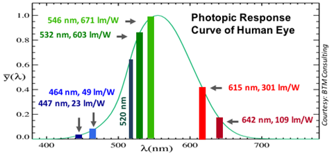
Finally, if output color /spectral width is precisely controlled, not only is color saturation improved, but less power is needed for the same perceived brightness vis-à-vis color sensitivity of the human eye:

For example, the preceding chart, taken from the projector industry but just as applicable to displays shows that if red were at 615 nm instead of the 642 nm commonly available, 66% less power would be still be perceived as the same brightness; similarly, for green at 546 compared to 532 nm, some 10% less power would be needed.
Summary
In sum, current micro-displays are neither sufficiently bright or efficient (low enough power consumption for untethered mobile apps) for next generation wearables, particularly for emerging stylish AR “eyewear.” Only emerging microLED technology, on the order of 103 intrinsically brighter than incumbent micro-OLED technology can meet the requirements for next gen micro-display; however, it emits largely in monochrome (blue/violet) necessitating downconversion to obtain RGB colors.
For a variety of technical reasons the industry is beginning to appreciate, traditional color downconverting methods used in SSL and larger displays such as phosphors or QDs will not work as sub-pixels shrink, particularly <10 µm. Only QWs offer a viable technical solution to the fundamental problems, yet have several manufacturing challenges.
Combining the QW approach with a novel resonator, however, simplifies matters, including in manufacturing, and allows near full absorption of the underlying microLED light in a very thin color converting layer overlaying or integrated with the microLED micro-display. This Chromover™ technology is further the only known scheme that can select for output wavelength and spectral width, and control directionality, offering the ability to confine the output within a narrower cone angle.
With the advent of sophisticated new, holographic and diffractive waveguide structures to convey micro-display imagery, sensitive to input angle and spectra, only such technologies can offer a solution for efficient color conversion in emerging microLED micro-displays.


