Toyohashi, Japan and Dresden, Germany – 3rd March 2021 – The team of Prof. Sekiguchi of Toyohashi University of Technology and ALLOS Semiconductors have engaged to realize high efficiency nitride-based micro LED chips for novel in-vivo neutral application.
Since their evolution in the 1990s, nitride LEDs have made inroads into our daily lives, saving energy and enabling many new applications. They are known for their ubiquitous use in numerous illumination applications and the emerging micro LEDs are famous in particular for use in super large TVs or groundbreaking augmented reality displays as well as robust automotive displays.
Nitride LED for medical application
Beyond the obvious illumination applications, nitride LEDs are also increasingly proving helpful in medical applications. For example, nitride LEDs emitting UV light are employed to fight viruses like COVID-19 by disinfecting surfaces.
Another example is Toyohashi University of Technology, Japan using nitride micro LED technology to build medical brain/machine interfaces. Prof. Hiroto Sekiguchi’s group has developed a neural probe to study brain functions using ALLOS’ micro LED epiwafer. To avoid brain damage, high-efficiency of micro LEDs is key in order to reduce harmful impact from heat coming from conversion losses. Furthermore, for micro LEDs extreme precision is needed.
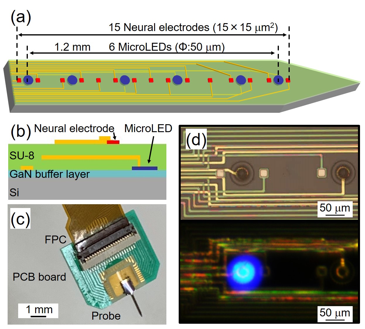
Figure 1: Micro LED neural electrode probe fabricated by Prof. Sekiguchi’s group integrating ALLOS’ high crystal quality and strain-engineering epiwafer technologies.
GaN-on-Si to overcome manufacturing challenges
For this novel medical application, manufacturing challenges had to been overcome, where ALLOS’ GaN-on-Si technology plays a key role. In particular, it was important to integrate nitride LED technology – the ‘GaN’ in the GaN-on-Si – with mature and precise silicon industry processes in order to achieve highest accuracy and reliability standards – the ‘Si’ in the GaN-on-Si.
Commenting on the challenges, Prof. Sekiguchi said: “We need to achieve extreme precision and reliable results. Only industry-grade silicon processing equipment – as we fortunately have at our university – can deliver such processing results. Thus, using ALLOS’ GaN-on-Si epiwafers which can be processed on silicon lines was the right choice.” Adding to Prof. Sekiguchi’s assessment, Dr. Atsushi Nishikawa, CTO of ALLOS said: “With our CMOS line ready GaN-on-Si technologies we unlock the benefits those silicon lines bring – including scalability to 200 and 300 mm for low cost and the exceptionally high reliability and yield levels required for all micro LED applications.”
Further information you can read in the article by authors from Toyohashi University of Technology and ALLOS Semiconductors in the Japanese Journal of Applied Physics (Jpn. J. Appl. Phys. 60, 016503 (2021)) and contact us directly.
About Dr. Sekiguchi at Toyohashi University of Technology
Dr. Sekiguchi has been working on the development of nitride semiconductor for more than 10 years. Currently he is considering micro LEDs as a new optogenetic tool for brain science. He and his research team are developing a new neural probe that has micro LED for manipulating neural activity and neural recording electrode for recording neural activity using their Si semiconductor process technology and ALLOS’ GaN-on-Si technology. They believe that such device development will be a powerful tool for opening up new field of neuroscience.
About ALLOS Semiconductors
ALLOS Semiconductors is the global leader for gallium nitride on silicon epiwafer technology (GaN-on-Si) for next generation, micro LED-based display solutions. Our customer and partner base includes top-tier companies from the electronic device, display, LED and semiconductor foundry industries. They benefit from the cost, yield and performance advantages of our patent-protected 200 and 300 mm GaN-on-Si micro LED epiwafers. These benefits are available to ALLOS’ customers through micro LED epiwafer supply, licensing, turn-key technology transfers and integration projects.
Source: ALLOS


