-
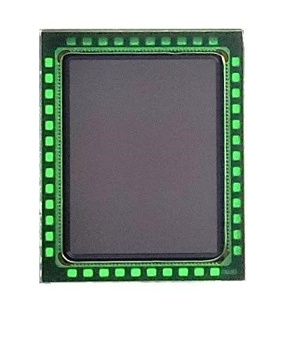
Compact Mira050 offers high sensitivity to light in the visible and NIR spectrum
-
Industry leading power consumption and high sensitivity requires less illumination to help extend battery run-time
-
Designed to bring power savings at high-quantum efficiency for smart glasses, VR headsets and other fast-growing consumer electronics applications

Premstaetten, Austria and Munich, Germany (6 January 2023) -- ams OSRAM (SIX: AMS), a global leader in optical solutions, today extended its Mira family of pipelined, high-sensitivity, global shutter CMOS image sensors with the launch of the 2.3mm x 2.8mm, 0.5Mpixel Mira050.
Highly sensitive to both visible and near infrared (NIR) light, the Mira050 enables engineering designers to save space and power in wearable and mobile devices. The Mira050 is suitable for applications such as eye tracking, gesture tracking and contextual awareness in AR/VR/MR headsets, object detection in robots and 3D depth sensing for face recognition in smart door locks.
The Mira050 is designed to pack high performance technology in a miniature package with numerous ultra-low power features. Power consumption is a mere 47mW even at full resolution and a frame rate of 120fps and stand-by power consumption is very low at 60µW. From a technical standpoint, Mira 050 delivers high sensitivity to visible and NIR light that is also matched by high quantum efficiency: from 36% at 940nm and 56% at 850nm in the NIR spectrum and up to 93% at 550nm in the visible light range based on ams OSRAM´s internal testing. The benefit is extra power savings, as the sensor can operate with a low-power illuminator as well as in naturally low-light conditions. On-chip power management additionally adjusts the power supplied to various functional blocks in response to settings for the frame rate and exposure time, helping to extend battery run-time even more.
The ams OSRAM engineers designed Mira050 to ease the development of high-performance imaging systems through features such as on-chip event detection and background light subtraction.
Jens Milnikel, Executive Vice President and General Manager BU Image Sensor Solutions at ams OSRAM, said: ‘In wearable and mobile devices, the most important parameters for an image sensor are active area utilization or footprint efficiency and power consumption. For both of these desired attributes, the Mira050 is a leader in the market, offering higher resolution, higher sensitivity and lower power consumption in a smaller footprint.’
Advanced pixel technology and unique architecture

In the Mira image sensor family, ams OSRAM uses back side illumination (BSI) technology to implement a stacked chip design, with the sensor layer on top of the digital/readout layer. This allows it to produce the Mira050 in a very efficient chip-scale package.
BSI technology also gives the sensor very high sensitivity and quantum efficiency with a pixel size of 2.79μm. Effective resolution of the chip-scale package is 576px x 768px and maximum bit depth is 12 bits, with a bare die version at 600px x 800px. The sensor is supplied in a 1/7” optical format.
Programmable registers enable the user to control window co-ordinates, timing parameters and exposure time, and mirror, flipping and cropping functions. The MIPI CSI-2 interface allows for easy interfacing with a processor or FPGA. On-chip registers can be accessed via a Camera Control Interface (CCI) for easy configuration of the sensor.
Sampling of the Mira050 NIR image sensor is expected in late Q1. More information about Mira050.


