2020-11-02
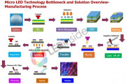
Mass Transfer Process Demonstrated as a Commercially Viable Method of Producing MicroLED Displays of any Size from Cellphones to TVs and In-between. VerLASE Technologies announced today substantial progress in demonstrating its novel mass transfer process, which is the key impediment to microLED displays industry realizing its full potential. The process is based on a unique technology being developed by the Company called the Photo-Mechanical Actuation (PMA). The company asserts its process once fully implemented is capable of very high transfer thr...
Continue reading →
 2020-03-13
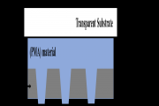
Micro LED technology builder VerLASE introduced a novel mass transfer technique for Micro LED display production based on its “Large Area Assembly Platform” (LAAP), which the company revealed in June, 2019. With similar concept, the company transfer the technology into a simpler, semiconductor-fab compatible solution based on Photo-Mechanical Actuation (PMA). According to VerLASE, the solution uses a novel formulation comprising of fab compatible chemistries and transfer stamp architecture in a unique way to deterministically pick-up a large ...
Continue reading →
 2019-04-22
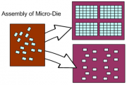
Micro LED start up VerLASE announce that it is developing unique technologies for massively parallel assembly of Micro LED dies or films to address the major challenge of Micro LED display mass production. VerLASE, a spin-off of Versatilis, aims to develop novel technology of color conversion layers for Micro LED display. The company focused on practical methods with semiconductor and MEMs industry methods and existing tools in novel ways to enable deterministic, massively parallel transfers of Micro die, yet with provisions that allow selective repair. A...
Continue reading →
 2017-11-23
Inorganic microLEDs are the next big thing in displays, not as backlights for LCDs, but like OLEDs, as the actual light emitting pixel elements, ranging from applications in Micro-displays for Augmented /Virtual Reality (AR/VR) to wearables such as Smartwatches and Cellphones. Unlike OLED displays, however, they are far more robust and long-lived, and most importantly, far more efficient and much brighter, making them viable even for larger displays, such as video walls in advertising and in cinema in place of projection. But to make the technology cost effective, manufacturing challenges abound, particularly as pixel sizes shrink in next generation micro-displays. For example, various coatings must be rapidly deposited in a precise, controlled manner, such as the Quantum Dots (QDs) integrated with the LEDs used in larger displays either to sharpen the color characteristics of traditional phosphors, or fully replace them in micro-displays, relying solely on QDs for color conversion. Better technology is needed for reliably depositing the various costly materials used, and even for rapidly assembling or arraying the microLEDs themselves.
Continue reading →
 2017-08-07
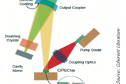
Augmented Reality (AR) is thought by many, including many of the leading CEOs in Silicon Valley, to be the “next big thing,” ultimately displacing our smartphones with stylish, interactive glasses that communicate with the digital world, in part by superimposing virtual images on the wearer’s field of view. Huge investment is pursuing this vision, much of it focused on micro-displays and sophisticated optics for overlaying images onto a wearer’s view. But just as promising is the idea of scanning such images directly into the human eye. Needed are very low power lasers or laser arrays in RGB or more colors that can be packaged in very small, discreet form factors suitable for integration into attractive, fashionable eyewear. Such lasers do not yet exist, but a technology that meets the challenge is in development, which can also lever the existing manufacturing infrastructure for LEDs. It can also address many other applications in emerging bio-tech and even in SSL markets for highly directional lighting.
Continue reading →
 2016-12-16
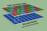
Color conversion is a challenge for micro-LEDs where pixels can approach sizes smaller than 5 microns, particularly in micro-displayapplications for mobile devices where overall size, as well as efficiency are all important. Traditional phosphors and even quantum dots (QDs) are not applicable to the micron sized LEDs, principally because of the thickness of material needed.
Continue reading →
 2020-03-13
 2019-04-22
 2016-12-16