 2018-12-21
Having looked back at the industry updates of Micro LED technology, let’s keep on reviewing the technology breakthroughs of Micro LED in the past year.
KAIST Team Develops Flexible Vertical Micro LED to Cure Hair loss Problem
In January, a researcher team at KAIST announced the development of flexible vertical micro LEDs (f-VLEDs). These f-VLEDs achieved optical power density (30 mW/mm2) three times higher than that of lateral Micro LEDs and can be applied to optogenetics for controlling the behavior of neuron cells and brains with...
Continue reading →
 2018-11-05
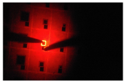
Micro LED displays require the use of red, green and blue (RGB) LEDs, achieved by mixing nitride LEDs and phosphide LEDs. This mixing causes blue, green and red LEDs to behave differently in terms of temperature and aging, which impacts the quality of image color. Moreover, blue, green and red LEDs each require specific electronic drivers, making integration more complex. (Figure 1: Red emission at 630nm of 100µmx100µm of full InGaN LED grown on Soitec’s InGaNOS) RGB LEDs composed of the same material inducing the same behav...
Continue reading →
 2018-02-09
LEDinside listed out companies worldwide that have tapped into the development of Micro LED and what they have achieved so far. This up-to-date table covers the majority of the activities happening within the global Micro LED developing force.
Continue reading →
 2017-10-17
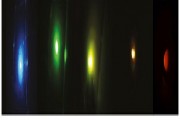
The ideal solution for microLED makers would be the availability of efficient nitride LEDs in both green and red. In this case, all RGB LEDs would be composed of the same material with the same behaviors and driving conditions. The challenge is to find one material capable of spanning the blue to red spectrum.
Continue reading →
 2014-11-20
In part one of EcoLightTech Asia 2014 Innovative Product guide, LEDinside addressed smart or innovative products displayed by Thai LED manufacturers. Here we will take a look at the interactive and smart LED products international manufacturers were showcasing at the lighting show that took place in Bangkok, Thailand recently.
Continue reading →
2013-12-20
Soitec and CEA have renewed their long-standing and fruitful partnership for the next five years. This new contract aims to support Soitec’s strategy for the electronics, solar energy and lighting markets. It will focus on engineered substrates and materials offering higher performances and energy savings at a competitive cost.
Continue reading →
2013-02-25
HVPE system expected to lower the cost of LED production and accelerate adoption in commercial and residential lighting GT Advanced Technologies (NASDAQ: GTAT) and Soitec (NYSE Euronext: SOI), today announced a development agreement and a licensing agreement allowing GT to develop, manufacture and commercialize a high-volume, multi-wafer HVPE system to produce high-quality GaN epi layers on substrates used in the LED and other growth industries such as power electronics. The higher growth rates and improved material properties made possible ...
Continue reading →
2013-02-22
Major step in joint partnership to develop market of GaN substrates for high-performance LED lighting applications. Soitec (Euronext), a world leader in generating and manufacturing revolutionary semiconductor materials for the electronics and energy industries, and Sumitomo Electric Industries, Ltd., a leading worldwide provider of compound semiconductor materials, have signed a licensing and technology-transfer agreement under which Sumitomo Electric will use Soitec’s proprietary Smart Cut™ technology to manufacture engineered gallium nitride (GaN) substra...
Continue reading →
 2012-07-10
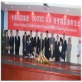
Chongqing Silian Optoelectronics Science & Technology Co., Ltd. (Silian) has cooperated with Soitec (Euronext) to jointly develop gallium nitride (GaN) template wafers using hydride vapor phase epitaxy (HVPE). And the partner companies plan to begin sampling GaN template wafers in 2012. The companies' joint development agreement aims at validating the manufacturability and enabling the commercialization of GaN template wafers using Silian's sapphire substrates and Soitec's unique HVPE technology. Chantal Arena, vice president and general ma...
Continue reading →
2010-12-02
Soitec and Sumitomo Electric Industries (SEI) has joined force to develop engineered gallium nitride (GaN) substrates.
The cooperation will combine with Sumitomo Electric's sophisticated GaN wafer manufacturing technology and Soitec's unique Smart Cut layer transfer technology.The engineered substrates retain the original, high crystalline quality of Sumitomo Electric's GaN wafer at a lower cost.
Continue reading →
 2018-12-21
 2018-02-09
 2017-10-17
 2014-11-20
 2012-07-10