Micro LED displays require the use of red, green and blue (RGB) LEDs, achieved by mixing nitride LEDs and phosphide LEDs. This mixing causes blue, green and red LEDs to behave differently in terms of temperature and aging, which impacts the quality of image color. Moreover, blue, green and red LEDs each require specific electronic drivers, making integration more complex.

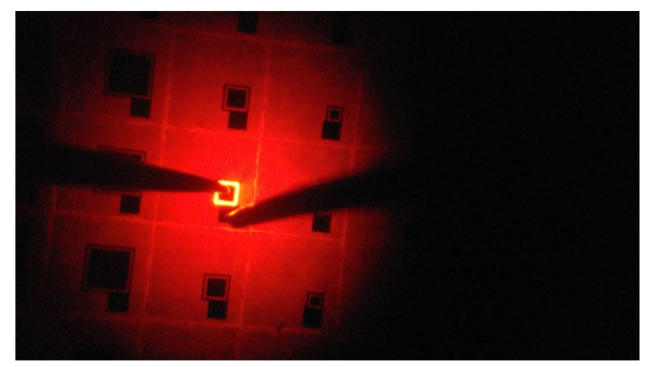
(Figure 1: Red emission at 630nm of 100µmx100µm of full InGaN LED grown on Soitec’s InGaNOS)
RGB LEDs composed of the same material inducing the same behaviors and driving conditions represent the ideal solution for microLED makers. The critical challenge is finding one material capable of spanning the blue to red spectrum. Theoretically, the indium-gallium-nitride (InGaN) alloy can cover the entire visible range by adjusting the indium content to fine tune the peak emission wavelength. However, high indium content in GaN-based LEDs results in poor quality because of lattice mismatches between the GaN buffer layers and the InGaN quantum wells.
Soitec’s relaxed InGaN based substrate
Soitec has developed an innovative substrate called InGaNOX (InGaN-on-X) that overcomes lattice mismatch. The substrate has a top relaxed InGaN layer that can be used as a seed layer for full InGaN LED growth. The technology was demonstrated last year in fabricating blue, green and amber nitride emitting heterostructures on a 100-mm wafer. (See Disruptive Substrate Technology for Direct Green and Red Micro LEDs) Since early 2018, Soitec, CEA-Leti, and CRHEA/CNRS have collaborated on the development of full InGaN red LED emitting to target 630nm.
Soitec’s InGaNOX substrate currently offers lattice parameters up to 3.205 Ȧ. Pattern size can be customized from square millimeters down to 5 µm x 5 µm. Specific handle substrates can be ordered such as glass, silicon or sapphire, including PSS sapphire.
Direct emission from full InGaN red LEDs
The benefits of relaxed InGaN substrates are demonstrated by the growth of full InGaN emitting heterostructures and their direct emission. These heterostructures have been grown and characterized by the electronics research institute CEA-Leti.
Full InGaN LED heterostructure is grown on InGaN-on-sapphire (InGaNOS) substrates with a lattice parameter of 3.205 Angströms. A conventional chip process has been then applied on the LED structure. The emission arises from the back side of the LED chip through sapphire. 3 LED patterns are designed inside the patterned epi wafer at 100µmx100µm (Figure 1), 50µmx50µm and 30µmx30µm.
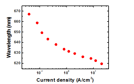
As shown in Figure 2, microLEDs exhibit a red emission from 620nm up to 660nm according to current density.

(Figure 2: Red emission of full InGaN-based versus current density for 50x50µm² chip size.)
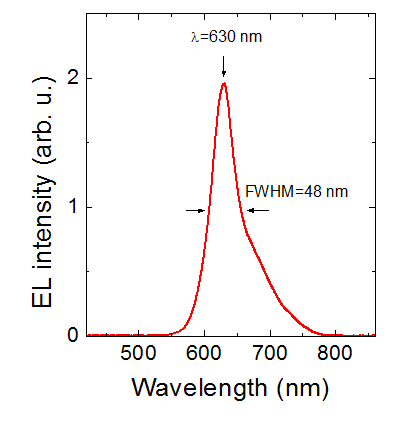
The resulting electroluminescence emission at 630nm has 48 nm FWHM at current density of 0.8 A/cm² as shown in Figure 3.

(Figure 3: Red emission of full InGaN-based LED grown on Soitec’s InGaNOS substrate.)
This pure red emission on full nitride LED proves highly promising and will lead next to focused research and development efforts on increasing EQE through LED structure development and InGaN film quality.
Innovative solutions from Soitec for microLED display makers
Soitec’s engineered substrate technology offers innovative solutions to the current challenges facing the microLED industry by eliminating the need for phosphor converts and nitride/phosphide LED mixing, through efficient nitride-based red LEDs with direct emission and enabling an enhanced color quality consistency with full InGaN blue, green and red LEDs.
Additionally, Soitec’s InGaNOX technology could be used to create substrates with mixed lattice parameters, enabling growth of different colored LEDs on the same substrate. This innovation can significantly reduce the cost of microLED mass transfer within microdisplay fabrication.
Aknowledgements
This work has been developed with the collaboration of CEA-LETI and CRHEA/CNRS. The authors wish to thank A. Dussaigne, S. Chenot and B. Damilano for their contribution.
For more information about Soitec’s InGANOX technology, please contact David Sotta Ph. D., Soitec Compound Product Manager, david.sotta@soitec.com.


