 2025-09-10
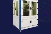
Eulitha AG, a provider of advanced photolithography solutions, announced a significant milestone as several Asian VCSEL (Vertical-Cavity Surface-Emitting Laser) foundries have adopted its DUV (deep ultra-violet) patterning platform for 6-inch wafer production. Eulitha has recently shipped multiple systems to support the rapidly growing demand for VCSELs used in applications ranging from LiDAR, 3D sensing, data centers, and next-generation optical communications. Eulitha will be exhibiting at CIOE September 10-12th and presenting on ‘Innovative o...
Continue reading →
2015-06-03
EULITHA, a Swiss startup company offering innovative lithography equipment and services for the nanotechnology, photonics and optoelectronic markets announced today the delivery of its unique PhableR 100 photolithography tool to the MESA + NanoLab of the University of Twente in the Netherlands. The system incorporating Eulitha’s proprietary Displacement Talbot Lithography technology will enable researchers of this interdisciplinary research institute to perform high resolution lithography on different substrates without the severely limiting requirements such as flatness or conductivity one faces with previously available technologies.
Continue reading →
2012-01-11
Eulitha AG, a pioneer and leader in the production of high-quality nanostructures using advanced lithography techniques, today announced that it has signed a joint-development and licensing agreement with EV Group (EVG), a leading supplier of wafer bonding and lithography equipment for the MEMS, nanotechnology and semiconductor markets. EVG will integrate Eulitha’s PHABLE™ mask-based ultraviolet (UV) photolithography technology with EVG’s automated mask aligner product platform with the goal of developing a low-cost-of-ownership (CoO) nanopatte...
Continue reading →
 2025-09-10


