In the past few years, Micro LED has proven to be a very promising display technology. At this point, the industry is preparing to transition from the prototype stage to mass production. Therefore, the focus is shifting to the two major challenges that slow down Micro LED display technology commercialization: the low yield and the high cost. How to optimize the production process efficiently in order to increase yield, while simultaneously reducing cost, is the most essential challenge for Micro LED technology developers at the moment.
As improving yield is a primary goal for most of the players in the industry, inspection has emerged as a critical factor in the process of Micro LED development. Developers and manufacturers are looking to identify defective pixels and other problematic sub-pixel features. Since the chip size of Micro LED can be as small as single-micron, much smaller than conventional LEDs, existing inspecting equipment is inadequate in many respects for Micro LEDs; many standard tools simply don’t provide high enough resolution. Moreover, with the smaller pixel sizes, there is also a dramatic rise in the number of pixels that need to be processed during inspection. As a result, inspection with advanced accuracy and higher resolution has become critically necessary in order for Micro LED displays to achieve commercialization.
What are the key points of Micro LED inspection during the manufacturing process and how can inspection equipment suppliers support this process? To answer these questions, LEDinside interviewed InZiv, an Israeli startup focusing on Micro LED inspection. David Lewis, CEO of InZiv, explained the fundamentals of inspection and the critical role it plays in advancing Micro LED mass production.
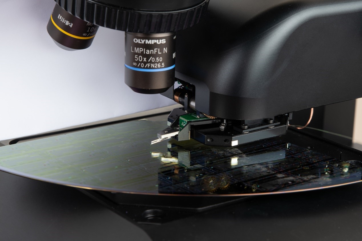
(Image: InZiv)
High-Resolution Inspection Process Combining PL and EL Testing Suitable for Single Micron Chips
There are two main ways to perform LED testing: photoluminescence (PL) and electroluminescence (EL). PL testing is based on optical excitation, while EL testing is based on electrical excitation. Both methods enable the user to inspect the LEDs and analyze that they are functioning properly and meeting industry standards and requirements.
Each method provides certain advantages. PL can test LED chips rapidly without any contact, but it might not detect all the defects. On the other hand, while EL is able to identify more defects, it tests LED chips by electrical excitation, which requires physical probing of the electrical contacts. Since Micro LED chips are extremely small, EL is becoming increasingly challenging.
The inspection solution of InZiv offers the highest optical resolution, and combines both PL and EL testing. It first conducts a large-scale wafer PL- scanning to identify the problematic areas or regions of interest (RoI). Then InZiv focuses on these identified areas to further examine them with high resolution PL testing, or nano-PL. The nano-PL is conducted using patented nano-optical technology, allowing for 100 nm resolution. Finally, nano-EL inspection is performed to complement the nano-PL by confirming the full operative functioning of the pixels.
“A typical Micro LED wafer may contain millions of pixels. This filtering process allows us to reduce the number of pixels that require high-resolution inspection, leaving a manageable number of pixels for EL testing,” explained Lewis. In this way, InZiv substantially improves inspection efficiency and enables more sophisticated cost management for inspection. Furthermore, functioning Micro LED chips need not be affected by any unnecessary testing.
Speaking of the accuracy of the inspection, Lewis provided a remarkable number: “Our inspection solution can go down to chip sizes of <1 µ with high accuracy (100nm) and high-repeatability (± 10%),” indicated Lewis.
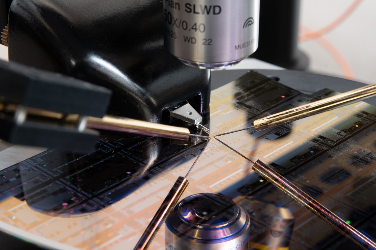
(Image: InZiv)
Correlated Characterization and Defect Review Library to Improve Manufacturing Process
An effective testing solution not only has to focus on inspection accuracy but also must provide a comprehensive approach to characterize a wide variety of chip sub-features that enables manufacturers to review their Micro LED production process for further enhancement.
Accordingly, InZiv addresses the various sub-features of Micro LED chips through high resolution correlated characterization, helping its clients review defects of chips and improve their process and production yield. Lewis said, “InZiv is offering a dedicated tool to both test devices and perform correlated defect review for the characterization of Micro LEDs at 10 times better resolution compared to existing technologies.” Micro LED producers can review different chip characteristics such as optical and spectral irregularities, nano-metric 3D structure, angular distribution, EQE and thermal measurements, as well as optically and structurally correlated side-wall measurements, so that they can further identify the fundamental issues of the manufacturing process and improve them accordingly.
With the inspection process covering PL wafer mapping as well as nano-PL and nano-EL pixel mapping, InZiv plans to integrate many additional data points in order to build up a database for a defect library.
By providing comprehensive details of Micro LED chips via the inspection and characterization processes, InZiv can help technology developers investigate their own process according to the results and focus on the problematic areas for efficient and effective optimization.
InZiv on the Move, Planning to Expand Inspection Equipment Portfolio to Different Phases of Micro LED Production
As Micro LED display technology is at the turning point evolving from prototype to mass production, InZiv believes that the demands for inspection will expand. “InZiv is designing a portfolio of inspection equipment to address the needs of the Micro LED world across all of its different strata,” highlighted Lewis.
He noted that InZiv is launching a pre-mass transfer full wafer inspection solution which is able to process a 6-inch wafer within 25 minutes with its large scale PL testing. The company is working on reducing the inspection time to under 15 minutes and aims to reach this goal next year. As for EL testing for pixels, InZiv is in the process of developing a rapid full wafer EL testing capability.
Apart from improving the speed of wafer inspection, InZiv is also in discussion with various suppliers for a post-mass transfer inspection solution. Lewis said the method can be deployed even down to the process of panel production.
“A principle goal at InZiv is to extend our current portfolio of instruments to better serve Micro LED production,” emphasized Lewis. Since Micro LED display technology is still developing, members of the industry are open to possible solutions and are enthusiastic to discover new techniques to achieve technological breakthroughs. The evolving environment allows InZiv to develop more collaborations within the supply chain.
InZiv is working with the leading Micro LED technology companies and has already received positive response from the clients. As the market continues to grow, InZiv is seeing exploding demand for its high-resolution inspection solution at every level of Micro LED technology development.
To learn more Micro LED technology breakthroughs and progresses as well as the ongoing market trend, join 2020 Micro LED Forum!