Author: Steven Chen, Process Control Solutions Technologist, KLA-Tencor Corporation
Introduction
LED manufacturing is undergoing a tremendous transformation. The evolution to high brightness LED, larger wafer size and new complex architectures make LED manufacturing more challenging than ever before. Even though these trends greatly benefit the advancement of the LED industry in terms of LED efficiency and performance, they can also potentially negatively impact yield. In order for LED manufacturers to stay competitive in this dynamic environment, they need to have a comprehensive in-line process control strategy to improve the yield to make the solution cost effective.
Currently, most LED manufacturers rely on inspection tools to inspect and provide defects of interest (DOI). Defect density is typically utilized as the gauge for statistical process control (SPC) control. However, the drawback of this approach is the fact that there can potentially be a lot of nuisance defect that does not cause yield loss. In looking at a defective wafer through an inspection tool, how do you determine which defects are killer defects that impact the yield or electrical performance, and which defects are nuisance? How can killer defects be detected at the earliest possible time to prevent costly excursions? These are the questions that must be addressed properly.
In-line monitoring is critical in determining how defects affect the yield and a proper strategy would have tremendous return on investment. Advanced defect and yield analysis solutions are needed to enable the process control loop. Further, the current method of using total defect density is impractical. A systematic methodology is introduced in this paper to identify yield-impacting defects and its relationship to yield.
Background and Purpose
First of all, it is crucial to distinguish yield-impacting defects from nuisance because not all defects impact the final yield specifically. This use case aims to understand the relationship between epitaxial defects and its impact on yield, as well as creating a systematic approach in separating yield-impacting DOI from nuisance. One such approach is to use the ‘kill ratio analysis’ which will be described further in this paper. In utilizing defect attribute binning with the kill ratio results, one will finally be able to observe the correlation to yield.
Methodology Overview
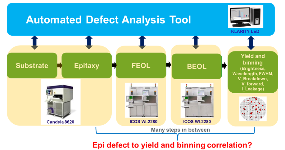
In order to establish a proper process control loop, advanced defect equipment such as that depicted in Figure 1 are needed. Defect information inspected from substrate, epitaxy, front-end of line (FEOL) and back-end of line (BEOL) can feed into an automated defect analysis tool. In this particular case, we are interested in learning whether the epitaxial defect correlates to yield.

Figure 1. In-line monitoring solution
The high level overview of the methodology is shown in Figure 2. After the data is gathered, we need to obtain accurate bin sort data, a list of wafers, yield information and defect types from the inspection tools. Then, we use the yield management software tool, such as KLA-Tencor’s Klarity LED, - to do the analysis. In this step, we need to ensure that the defect map aligns with the bin sort map accurately. It is crucial to have an accurate wafer alignment because it is the basis of the kill ratio analysis. Using this kill ratio information, we can derive the yield-impacting DOI definition. Once we have obtained the DOI definition, we can apply it to all wafers. Upon finishing the kill ratio analysis, we perform data analysis to identify yield-impacting defects by correlating the defect counts to the final bin yield. Lastly, we will obtain trend charts and be able to set upper control limits and SPC controls. The analysis is repeated until the yield-impacting DOI definition is satisfied.

Figure 2. Analysis methodology
Kill Ratio and Terminologies
Kill ratio represents a proportion of defects estimated to cause die failure. It is also derived from past data. It is used to find the amount of defects on a current inspection that will cause die failure at the end of the process. It can help to determine the disposition of problem wafers or lots.
In order to understand how kill ratios work, we need to understand the kill ratio model terminology. First, bin data represents good or bad die from bin code. The bin data is typically provided by the LED manufacturer. In addition, the defect data separates clean or dirty dies from adder defect location. A clean die contains no detected adder defects while a dirty die contains detected adder defects. Figure 3 illustrates this concept. The square boxes represent dies. The dots represent defects. Green boxes indicate good dies while white boxes indicate bad dies. Therefore, good clean dies means good dies without defects. Good dirty die mean good dies that have defects. Furthermore, we also have total clean dies and total dirty dies which are self-explanatory from the names. Figure 4 depicts yield and kill ratio formulas.

Figure 3. Bin data and defect data illustration

Figure 4. Yield and kill ratio formula
Example and Experimental Results
Figure 5 below is an example of the yield study and correlation results to illustrate this advanced defect identification methodology. In the example below, assume that we are given 20 wafers with yield information and that the baseline yield is 76.25%.

Figure 5. Fictitious yield information used for illustration
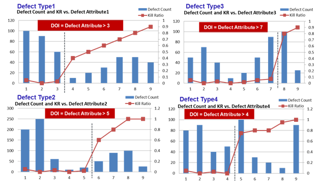
Layer, class, size, wafer zone, in-die region and signature membership are a few examples of defect attributes that can be analyzed. Here, we take defect size as the attribute under study and while Klarity LED was used to determine yield-impacting defects with defect size. Figure 6 illustrates how we determine the yield-impacting defect attribute for each defect type. Starting with a certain defect type, the defect count and the kill ratio with respect to its defect size was plotted. A dotted threshold line was drawn whenever sudden kill ratio jumps appear. In the case of defect type 1, its defect size is greater than three. The same experiment goes for defect type 2, defect type 3 and defect type 4. Essentially, the defect size binning is based on kill ratio threshold number. Potentially, one can have as many segments as one likes in order to see the impact of the yield with any defect size combinations.

Figure 6. Kill ratio study
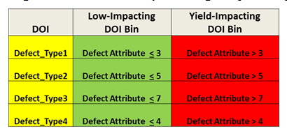
After performing kill ratio analysis on all defect types, the final yield-impacting DOI definition is shown in Figure 7. Bin 1 indicates a low-impacting DOI bin and bin 2 shows yield-impacting DOI bins which contain killer defects.

Figure 7. Yield-impacting defect of interest definition
The next phase of the analysis is to apply the yield-impacting DOI definitions to each wafer analyzed. Ultimately, we need to sum up all yield-impacting defects and see how well they correlate with the final yield. Twenty wafers with their total number of yield-impacting defects and total defects are shown in Figure 8. With respect to total defects, you can see that they do not correlate to yield well. For example, if one sets the upper control limit at 1400 defect counts, three wafers have defect counts greater than 1400. These are the wafers that contain the most defects; however, their yields are relatively high compared to the baseline average yield of 76.25%. This means that a lot of those defects do not translate to yield loss. On the other hand, if one sets the upper control limit (UCL) with a 1000 defect count to yield-impacting defects, again, three wafers have more defect counts than 1000. Interestingly, their yields are a lot lower than the average. They average 16.25% below the baseline yield. As a result, one does not find wafers with high yield-impacting defect counts with high yields. This further solidifies this methodology.

Figure 8. Yield-impacting defects vs. total defects
Furthermore, two correlation charts using these twenty wafers are shown in Figure 9 below. The top graph compares yield vs. total defect counts, and the bottom graph plots yield vs. yield-impacting defect counts. The bottom graph makes more sense because it shows that as the yield-impacting defect counts increase, the yield decreases.

Figure 9. Correlation (total vs. yield-impacting defects)
SPC control on yield-impacting defects can be established based on the findings.
Figure 10 shows that wafers with high total defect counts do not translate to low wafer yield. With an UCL of 1400 defects, only one out of three wafers corresponds to below average yield. There is no correlation between total defects to yield. Therefore, one will be blind-sided if SPC is set based on total defect counts.
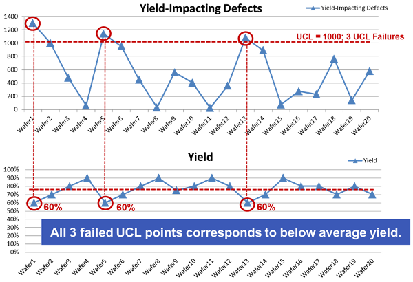
On the other hand, Figure 11 shows that high yield-impacting defects translate to low wafer yield. For example, with UCL of 1000 defects, all wafers that failed this control limit have below average yield. Therefore, SPC control can be established.

Figure 10. SPC monitoring with total defects

Figure 11. SPC monitoring with yield-impacting defects
Summary
In conclusion, in-line monitoring is critical to the LED manufacturing process. Separation of yield-impacting defects from nuisance defects is demonstrated with this monitoring methodology. The study shows that the kill ratio correlates with defect attributes such as defect size. Therefore, kill ratio analysis provides important guidance in setting defect attribute binning to identify yield-impacting defects.
Moreover, the defect to yield correlation methodology provided in this paper can help LED manufacturers to learn more about the yield relevant defect systematically. The LED manufacturers can implement SPC control to avoid expensive excursion and to realize the return on investment.
About the author
Steven Chen is a technologist within the Process Control Solutions group at KLA-Tencor. He has fifteen years of experience in the semiconductor industry. His experience encompasses a wide range from hardware design to application and semiconductor yield improvement. Steven holds an electrical engineering degree from Cornell University and an MBA from Santa Clara University.


