Photonic integrated circuits (PICs) are optical microchip systems with optical components utilizing light (or photons) for data transmission instead of electrons, which are the basis of traditional integrated circuits (ICs), also known as electronic integrated circuits (EICs).
This fundamental shift from electronic to photonic signals enables data to be transferred at the speed of light, resulting in significantly higher speeds and greater bandwidth compared with EICs, which are limited by the slower movement of electrons. Massless photons can transmit without the same resistive losses as EICs, leading to less power consumption and heat generation. PICs are also immune to electromagnetic interference due to the utilization of light. These features enable scaling and improvement of data transmission with high reliability.
Silicon photonics is a specialized field that integrates photonic components on a silicon substrate, creating sophisticated optical systems. These systems leverage the properties of silicon and other materials, such as silicon nitride (SiN) and silicon-on-insulator (SOI) wafers, to achieve high-performance optical components, such as waveguides and modulators.
Unlike electronics, where transistors are usually considered the basic functional cells, PICs don’t have a dominant component. Silicon photonics may include components such as lasers, waveguides, modulators, photodetectors, couplers, switches, resonators and multiplexers/demultiplexers, making the design and fabrication of PICs more complicated.
In addition, photon transmission does not rely on solid media such as electricity flow. Therefore, it is possible to travel through free space, such as applying LiDAR to detect the actual scene in 3D and create 3D point clouds for various use cases.
Why PICs and silicon photonics are gaining attention
The rise of AI and the growing demands of data centers have significantly attracted attention toward PICs and silicon photonics. These technologies enable high-speed data transmission, which is essential for supporting the massive data rates required by AI accelerators and modern data centers. AI’s rapid growth is driving the need for efficient, high-bandwidth communication, positioning PICs and silicon photonics as critical components in the future of AI and data infrastructure.
The primary driver for the development of PIC transceivers will be the escalating performance requirements of AI accelerators. As AI models and datasets grow in complexity and size, the demand for higher-performance transceivers will increase. The major driver in the near term is expected to be the demand for photonic transceivers in AI.
Advancements in materials for silicon photonics
Silicon photonics leverages the semiconductor properties of silicon to create PICs for various applications. The primary materials used in silicon photonics are silicon, silica (glass) and those chosen to address the inherent limitations of silicon.
SiN is widely used for passive components in silicon photonics due to its low optical loss and broad wavelength range. SiN is ideal for creating waveguides and other passive devices that require high optical power handling. Additionally, SOI wafers are the foundational material for many silicon photonic devices, providing strong light confinement and enabling the integration of multiple photonic components on a single chip.
Lasers are crucial for generating light in silicon photonics, and these lasers can be integrated into silicon photonic chips through various methods, including flip-chip bonding, heterogenous integration and epitaxial growth of III-V materials on silicon substrates. Complementary CMOS processing and semiconductor advanced packaging provide improvement in terms of laser integration, which is also considered to be the major focus. However, the material system of lasers for silicon photonics is still based on III-V compound semiconductors, such as indium phosphide (InP), due to silicon’s indirect bandgap.
In terms of modulators, traditional silicon modulators use the plasma dispersion effect, which, while effective, suffers from limitations in efficiency and insertion loss. Emerging materials, such as barium titanate and thin-film-lithium-niobate-on-insulator, are being explored due to their Pockels effect, which allows for high-speed modulation with lower drive voltages and higher bandwidths.
Photodetectors in traditional optical modules often use III-V materials such as InP. However, silicon photonics is moving toward silicon-germanium (SiGe) detectors, which can be integrated more seamlessly with silicon photonic circuits. SiGe detectors are particularly effective for high-speed applications and offer the advantage of being compatible with standard CMOS processes, thus reducing costs and simplifying manufacturing.
Emergence of co-packaged optics
The ever-increasing demand for higher bandwidth as well as fast transmission speeds, especially in telecommunications and data centers, has motivated the advancement of silicon photonics and PICs.
Traditional electronic interconnects, such as copper Ethernet, have reached bandwidth and power consumption limits over longer distances. The higher energy efficiency of data transfer has been realized by fiber optics and optical transmission, initially over long-haul networks and now within the data center infrastructure to increase efficient connections in network architectures.
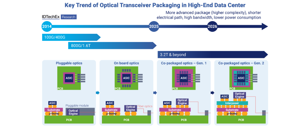
Optical fiber cables use pluggable optical modules containing an optical engine (OE) to convert optical signals to electrical signals and vice versa. These pluggable modules employ an electrical interface to connect the module with the switch/router ASIC in the network device by being inserted into a connector, which is mounted to the edge of a printed-circuit board and to the front panel of a network device.
PICs have already been adopted in datacoms and telecoms. The industry has already experienced a transition from pluggable optical transceivers to on-board optics, whereby an OE and switching chip are assembled on the same system board. One of the latest trends is the transition to co-packaged optics (COP), whereby OE is integrated in the same package as the switch ASIC to tackle limitation issues in performance, power consumption and size. This shortens the distance of high-speed electrical Serializer/Deserializer (SerDes) links to a few millimeters, thereby reducing the overall power consumption and heat generation of the I/O, significantly reducing latency, increasing bandwidth density and improving signal integrity.
COP reduces the transmission distance for electrical signals, resulting in enhanced performance and lower power consumption. This integration is especially beneficial for high-density ICs and is a significant trend in the industry, considering the continuously increasing data rates.
In traditional designs, optical transceivers are pluggable modules that connect to the switch ASIC via relatively long electrical traces.
COP technology can be used in Ethernet switches to support higher data rates. It integrates optical components directly with the switch ASIC within a single package, achieving higher throughput with lower latency and power consumption.
Advances and trends in integration methods
The integration methods in silicon photonics are evolving rapidly. In general, three integration methods are the most talked about:
-
Monolithic integration involves fabricating photonic active and passive elements directly on a single substrate in a unified manufacturing process.
-
Heterogeneous integration involves bonding or attaching elements fabricated from different substrates onto a single substrate. The elements may be based on different materials or varied manufacturing processes with distinct properties. Both monolithic and heterogeneous integration occur at the wafer or chip level. Techniques such as die-to-wafer and wafer-to-wafer bonding are usually utilized.
-
Hybrid integration happens at the package or board level. It involves assembling separate chips or modules into a single photonic system. These chips or modules are typically linked via optical interconnects.
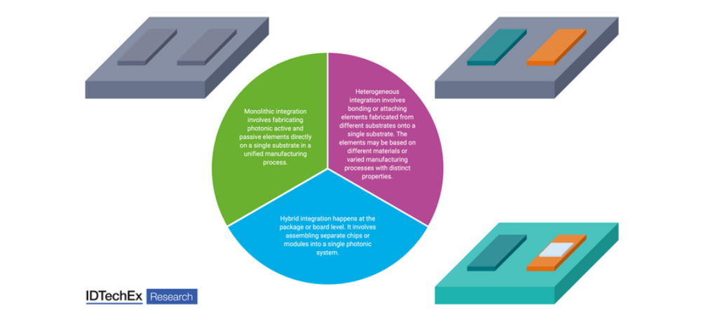
Three integration methods (Source: IDTechEx)
The trend toward large-scale integration and very large-scale integration in silicon photonics aims to increase the number of components on a single chip, enabling more complex and capable systems. This scaling is essential for applications in data centers, high-performance computing and advanced sensing technologies. In addition, advances in packaging techniques, such as photonic wire bonding and passive alignment methods, are improving the efficiency and scalability of silicon photonics. These techniques are essential for reducing insertion losses and enhancing the reliability of photonic systems. Also, integrating active components such as lasers and modulators on the PIC platform is currently a vital focus. All of these trends require the proper selection and further development of integration methods.
PICs and silicon photonics are at the forefront of technological innovation, transforming how data is processed and transmitted. By leveraging the unique properties of light, these technologies offer unparalleled speed, bandwidth and efficiency, making them essential for the future of AI, data centers and HPC. As advancements in materials, integration methods and packaging techniques continue, the potential for PICs and silicon photonics will grow, driving innovation and performance in various high-tech applications.


