Researchers based in China report the growth of high-brightness green indium gallium nitride (InGaN) light-emitting diodes (LEDs) on silicon (Si) [Haifeng Wu et al, Light: Science & Applications, v13, p284, 2024]. The epitaxial material was fabricated into normal-size LEDs and arrays of 5μm pixels at 7.5μm pitch in a 1080x780 format. A 30x30 array reached a brightness of 1.2x10⁷cd/m2 (nits) at 1000A/cm2 current injection, claimed as the highest reported for such micro-LEDs.
The research team from Hunan University, Innovision Technology (Suzhou) Co Ltd, Lattice Power (Jiangxi) Corp., Central South University, Beijing Digital Optical Device IC Design Co Ltd, and Hunan Normal University, sees the green portion of the spectrum as particularly important for “accurate color reproduction and overall image quality”.
Micro-LED displays are seen as key next-generation visual interfaces with immediate applications in virtual/augmented-reality contexts.
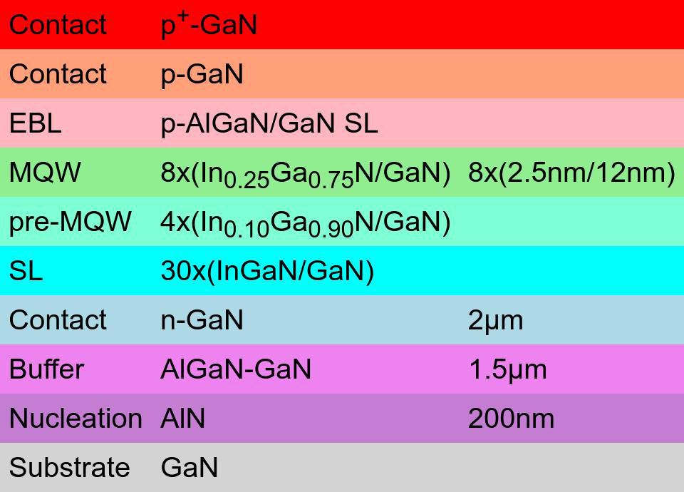
Figure 1: Epitaxial structure of green LEDs.
The researchers grew the green LED InGaN epitaxial material (Figure 1) using metal-organic chemical vapor deposition on Si (111) wafers. The large thermal expansion and lattice mismatches with GaN was bridged with a 200nm aluminium nitride (AlN) nucleation and 1.5μm AlGaN-GaN buffer layers. The buffer contained strain-control and dislocation-annihilation layer stacks.
The team sees the AlN nucleation layer as being critical for avoiding cracking of the materials that occurs when GaN is grown directly on silicon from thermal expansion mismatching between the layer and substrate. The best quality AlN is grown around 1400°C, which is dangerously close to the 1414°C melting point of silicon. Instead, the researchers used Ga as a surfactant to enable AlN growth at a lower temperature.
The researchers comment: “This approach promoted the migration of aluminum (Al) adatoms at a more moderate growth temperature of 1100°C by passivating the growth surface, thereby ensuring the subsequent growth of high-quality epilayers.”
The LED structure included a superlattice (SL) and pre- and green-multiple quantum well (MQW) structures, along with an electron-blocking layer (EBL) and n/p contact layers. According to the team, the pre-MQW structure “plays a crucial role in enhancing the quality and uniformity of MQWs with higher indium concentrations, especially for green light emission.”
The structure is credited with giving the main green light-emitting MQW a well-defined periodic distribution of indium with sharp InGaN/GaN interfaces.
X-ray analysis gave an estimate of 5.25x10⁸/cm8 for the total dislocation density. The convex bowing of the 4-inch diameter wafer was just 16.7μm at room temperature. The researchers credit the low bowing to “the meticulously engineered strain-control stacks”. A 6-inch wafer subjected to the same process also had a bow of 16.7μm, according to a supplementary report associated with the paper.
The team comments: “The small wafer bow rendered it highly compatible with subsequent standard wafer-scale fabrication processes such as wafer bonding and photolithography.”
A photoluminescence map showed a dominant wavelength of 531.98nm with a standard deviation of 0.939nm. The researchers add: “Notably, the wavelength variation across the wafer was 6nm and reduced to only 1.7nm at the 0.39-inch scale.”
LEDs (660μmx660μm) from the material demonstrated a 45% external quantum efficiency (EQE) at 30A/cm2 current injection, similar to the performance of corresponding-sized commercial devices on patterned sapphire.
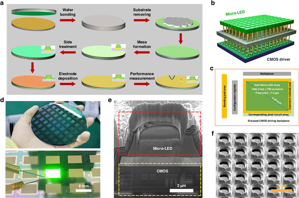
Figure 2: a Micro-LED fabrication process. b 3D integrated micro-LED chip matrix structure. c Layout of display. d Photograph of 4-inch wafer integrating multiple 0.39-inch green micro-LED displays. e Cross-section of pixel. f Three-dimensional structure of chips.
The researchers also fabricated micro-LED arrays (Figure 2), beginning with adding layers of 110nm sputtered indium tin oxide (ITO) and 700nm of chromium/platinum/gold to the epitaxial wafer. The wafer was then bonded to the CMOS drive chips without the need for alignment.
The researchers comment: “This approach overcomes the alignment accuracy limitations typically associated with thermocompression bonding equipment, enabling the fabrication of higher-resolution micro-LED chips.”
The epitaxial growth substrate was then removed.
Mesa formation was a three-step etch process removing the buffer layers, etching down to the metal bonding layers, and finally removing the metal stack with ion-beam etching. The mesa regions were protected by a silicon dioxide hard mask.
Sidewall defect repair and particle removal consisted of potassium hydroxide (KOH) treatment that acted anisotropically on sidewalls and top display surface of the micro-LED structure.
“This treatment not only removes residual materials from the sidewalls but also roughens the GaN grains on the mesa surface, facilitating photon escape from the chip,” the team writes.
Surface passivation consisted of a 50nm atomic layer deposition (ALD) aluminium oxide (Al2O3) coating.
The device was completed with window-opening to expose the n-GaN top layer, and deposition and patterning of the cathode and other metals for interconnection to the drive circuitry.
The researchers comment: “These micro-LEDs can be easily manufactured and integrated on a large scale as required.”
The up to 1080x780-pixel 0.39-inch displays included pixel array and peripheral circuits. A 30x30-pixel device had a high 108 rectifying ratio, 2.1V turn-on voltage, and 2.15 ideality factor. The turn-on voltage is considered to be low relative to the typically reported 2.5–2.8V.
The emission wavelength shifted as the injection current increased: 530nm to 505nm as between 0.3mA and 900mA, respectively. The shift is seen as resulting from piezoelectric and band-filling effects.
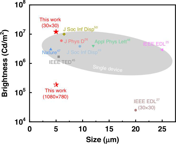
Figure 3: Comparison of micro-LED key parameters with typical reported results.
The brightness of a 30x30 array reached 1.2x10⁷cd/m2 (nits) at 1000A/cm2 (Figure 3). The larger 0.39-inch device managed 186017cd/m2 at 5A/cm2. The peak EQE of the 0.39-inch display reached 7.17% at 2A/cm2.
At 1.5A/cm2, the brightness standard deviation across the 0.39-inch display was less than 720cd/m2 about an average of 32,987cd/m2.
The researchers comment: “This exceptional brightness uniformity can be attributed to the uniform GaN-on-silicon epilayers and advanced fabrication technology.”
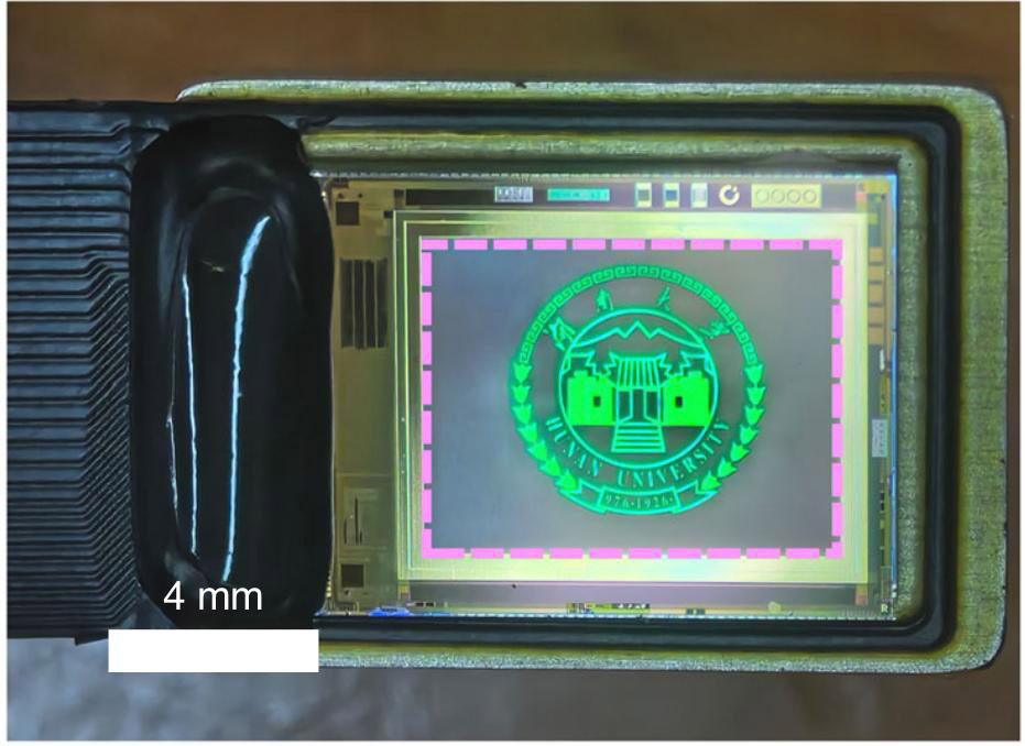
Figure 4: Packaged micro-display.
The packaged 0.39-inch displays had an 8-bit grayscale capability, enabling image and movie playback with contrast control (Figure 4).
TrendForce 2024 Micro LED Market Trend and Technology Cost Analysis
Release: 31 May / 30 November 2024
Language: Traditional Chinese / English
Format: PDF
Page: 160-180
|
If you would like to know more details , please contact:
|


