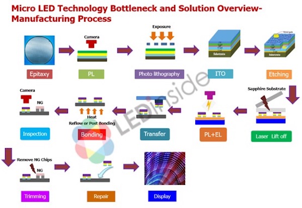
Despite that more and more industry players across the world have built partnership and poured resources into Micro LED development and research, the commercialization of the next generation display technology is still delayed. Due to technology barriers and equipment limitation, production cost for Micro LED display remains sky high, leading to postponed timeline of Micro LED display commercialization.
But why is the manufacture of Micro LED display so difficult? What are the challenges occurred during Micro LED production that slow down the commercial progress? LEDinside continues to investigate and observe the development of Micro LED technology and has identified the obstacles within Micro LED manufacture process.

In comparison with conventional LED, the demands for Micro LED is more complicated and sophisticated since Micro LED chip size is only 1% of LED, which is less than 100 um. The extreme size of the components marked a new generation technology and also brought about numerous new challenges. Here, we would like to analyze the process of Micro LED display production and point out the barriers of different steps.
Same as LED, epitaxy wafer plays a fundamental role in Micro LED chips. However, the requirement of Micro LED epitaxy is much higher than conventional LED. Given that chip size of Micro LED is no bigger than 100 um, the wavelength uniformity of epitaxy become even more critical as wafer unevenness could lead to defect of LED chips. However, currently most of the existing equipment was designed for conventional LED wafers production and can hardly meet the demands for Micro LED wafers.
Chip process on epitaxy wafer is also crucial as it would affect further production process including bonding and transferring. In order to meet the requirements of different transferring methods, chip makers would have to work closely with transfer technology providers for improve overall yield and efficiency.
To turn LED chips into a high performance display, Micro LED chips first need to be removed from sapphire substrate to a temporary substrate then from the temporary substrate to different backplanes depending on function and purpose required. Since the numbers of chips are massive and the size is incredibly small, the transferring process is very challenging. Conventional pick and place process will take too much time transferring millions of LEDs, boosting manufacture cost. Other transferring technologies are also in development to speed up the process. Moreover, bonding and assembling chips accurately on targeted receiving substrates without damaging the chips is a key challenge as well.
In addition, it is necessary to check functions of Micro LED chips during each of the manufacturing process to assure efficiency and enhance overall yield. When defects are detected, corresponding repairing technology to precisely address the defect is also a must. However, the difficulties of these processes still lay on the miniaturized chips. Equipment makers and solution providers have dedicated themselves to create more efficient and accurate approaches to tackle these issues.
Apart from the challenges within the production process, backplane materials, full color solutions and driver IC design are also part of the bottlenecks for Micro LED display manufacture.
To overcome the technology barriers, industry players have formed vertical integration and strategic partnerships in the supply chain to leverage their expertise with more holistic approaches. These collaborations have led to several technology breakthroughs announced in 2019, bringing Micro LED display a step forwards real world applications. However, technology developments addressing the difficulties of production processes are still inevitable for Micro LED commercialization.
This year, LEDinside will also invite worldwide experts in the industry to share their insights of Micro LED technology. Do not miss the opportunity to learn the latest trends and development of the next generation display technology!


 CN
TW
EN


