‘Downscaling’, the process of making elementary devices smaller in size, is at the heart of many technological breakthroughs in computing, information display, and human-machine interactions. For example, the downscaling of transistors has accelerated the speed of computers following the Moore’s law.
Similarly, the down-sizing of LEDs based on III-V semiconductors led to the invention of micro-LEDs, which are considered as an ‘ultimate technology’ for displays. However, micro-LEDs are very expensive to make as they require costly processes involving epitaxial crystal growth and mass transfer. Importantly, they exhibit severe efficiency losses when the pixel sizes reduce to ~10 microns or below, hindering their potential in commercial applications.
Recently, researchers at Zhejiang University and their collaborators at the University of Cambridge showed that it is possible to make extremely small LEDs based on perovskite semiconductors, reaching a new size limit not achieved before with conventional LEDs. They created micro- and nano-perovskite LEDs (micro/nano-PeLEDs) with characteristic pixel lengths from hundreds of microns down to 90 nanometers. For their green and near-infrared PeLEDs, high external quantum efficiencies of ~20% are maintained across a wide range of pixel lengths (650 to 3.5 microns). Unlike the conventional micro-LEDs based on III-V semiconductors, the micro/nano-PeLEDs exhibit minimum performance reduction upon downsizing. The nano-PeLEDs with pixel lengths of 90 nanometers are the world’s smallest LEDs, enabling a record-high pixel density of 127,000 pixels per inch (PPI) amongst all classes of LED arrays.
The related research paper entitled “Downscaling micro- and nano-perovskite LEDs” was recently published in Nature (Lian et al, Nature (2025), https://doi.org/10.1038/s41586-025-08685-w). The corresponding authors of the paper are Prof. DI Dawei and Prof. ZHAO Baodan of Zhejiang University. The first authors of the paper, LIAN Yaxiao, WANG Yaxin, YUAN Yucai and REN Zhixiang, are PhD students of Zhejiang University. Their collaborators include Prof. Samuel Stranks and Dr. Kangyu Ji of the University of Cambridge.
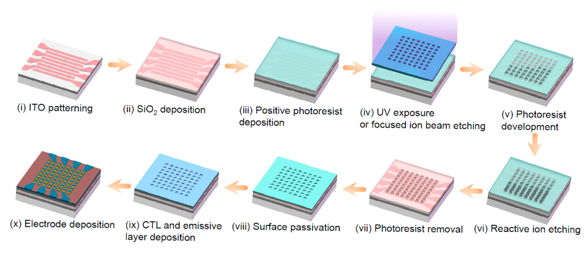
Figure 1: Fabrication processes of micro- and nano-PeLEDs. Source: Nature (2025).
“Making electronic devices smaller is an everlasting pursuit for scientists and engineers”, said Prof. DI Dawei, Deputy Director of the International Research Center for Advanced Photonics of Zhejiang University. “Perovskite LEDs are an emerging technology for display and lighting applications. Several years ago, we thought it might be a good idea to make perovskite LEDs smaller, similar to what has been done for micro-LEDs and micro-OLEDs. In 2021, we introduced the concept of ‘micro-perovskite LEDs (micro-PeLEDs)’. Since then, we wanted to make the devices even smaller, and explore the downscaling limits for the LEDs”, said Di.

Figure 2: Near-infrared micro- and nano-PeLEDs. Source: Nature (2025).
“Currently, the most advanced technology for display applications is micro-LEDs”, said Prof. ZHAO Baodan of Zhejiang University. “Micro-LEDs are based on III-V semiconductors. They are the best light source for augmented reality (AR) and virtual reality (VR) applications. However, the efficiency of micro-LEDs drops rapidly when the pixel sizes are smaller than 10 micrometers, which are the desirable pixel sizes for high-end AR/VR applications with ultra-high resolutions. Halide perovskites are a new class of semiconductors. It would be interesting to see how perovskite LEDs perform when they are made extremely small,” said Zhao.

Figure 3: Red and green micro- and nano-PeLED pixel arrays. Source: Nature (2025).
LIAN Yaxiao, the first author of the paper, is a PhD student supervised by Profs. Di and Zhao. He said: “Conventional photolithographic processes are not suitable for the direct patterning of the perovskite layers– it would damage the perovskite materials, so that we have to pattern the other functional layers instead.” “The simplest way of creating microscale perovskite LEDs is to pattern the top and bottom electrical contacts, so that the overlapping areas define the active pixels. However, this process leaves the perovskite materials at the pixel boundaries exposed to the electrode edges, creating non-radiative losses which reduce the LED efficiency”, said Lian. “This problem is overcome by our localized contact fabrication scheme, which uses lithographically patterned windows in an additional insulating layer to keep the active pixels away from the edges of the electrodes”,said Lian.

Figure 4: Efficiency of micro- and nano-PeLEDs versus pixel length. Source: Nature (2025).
“This new method allowed us to create micro- and nano-PeLEDs with pixel sizes ranging from hundreds of microns down to 90 nanometers”, said Lian. “For our green and near-infrared perovskite LEDs, external quantum efficiencies of ~20% are maintained for pixel lengths from hundreds of microns down to 3.5 microns.” For these LEDs, the downscaling effects start to pronounce at a very small size of about 180 nanometers, where the efficiencies of nano-PeLEDs reduce to half of the highest values. This suggests that at very small length-scales, the micro- and nano-PeLEDs are more efficient than III-V semiconductor-based micro-LEDs for which efficiency drops significantly at sizes below 10 microns. The size of the nano-PeLEDs were down to 90 nm, which are the smallest LEDs reported to date. This allowed the researchers to create an LED pixel array with an ultrahigh resolution of 127,000 PPI, a record-high resolution for all classes of LED arrays.

Figure 5: Images from an active-matrix micro-PeLED display. Source: Nature (2025).
Exploring the downscaling limits of these LEDs stemmed from the curiosity of the research team. But real-world display applications require LED arrays to be driven by a programmable circuit to deliver useful information. To do this, the research team has started working with LinkZill, a Hangzhou-based tech company commercializing thin-film transistor (TFT) technologies. They jointly created a prototypical active-matrix micro-PeLED display driven by a TFT backplane, capable of showing complex images and video clips. “We are excited to see the exceptional potential of the micro/nano-PeLEDs as a next-gen light source technology for display and beyond”, said Di.
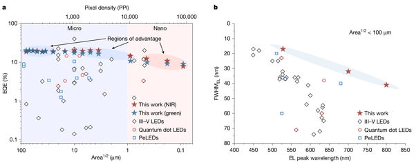
Figure 6: Comparing micro- and nano-PeLEDs with other LED technologies. Source: Nature (2025).
TrendForce 2024 Micro LED Market Trend and Technology Cost Analysis
Release: 31 May / 30 November 2024
Language: Traditional Chinese / English
Format: PDF
Page: 160-180
|
If you would like to know more details , please contact:
|


