-
Seoul Semiconductor Develops and mass produces Wicop which overcomes the incompleteness of CSP derived from silicon semiconductors
-
No need for main parts such as lead frame, gold wire, etc. and main packaging equipment such as die bonding, wire bonding, etc.
-
Burden will increase on LED companies that invested heavily in packaging processes due to commercialization of Wicop
-
As Seoul Semiconductor has already secured the global patent portfolio related to Wicop, it will take a close look at what the market will go, including the similar products.
 |
|
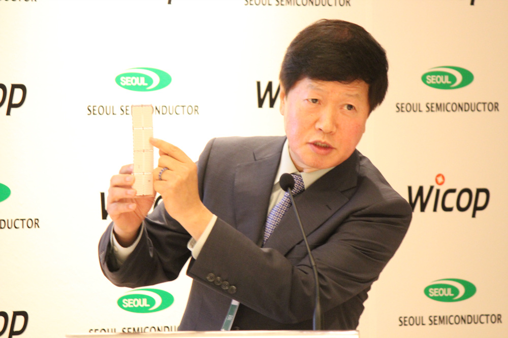
Seoul Semiconductor CEO Chunghun Lee introducing the company's new package free LED product Wicop LED at Pudong Marriot Hotel, Shanghai, China. (All photos courtesy of Seoul Semiconductor) |
On September 15th at Pudong Marriott Hotel, Shanghai, China, the global Seoul Semiconductor specializing in LED (CEO Chunghun Lee, www.seoulsemicon.co.kr) announced a new product, or the new concept Wicop LED which does not need processes such as Die Bonding, Wire Bonding, etc. which were necessary for the conventional LED Package production nor main LED package component parts such as Lead frame, Gold wire, etc.
 |
|
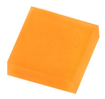
Seoul Semiconductor's new package free LED product Wicop LED.
|
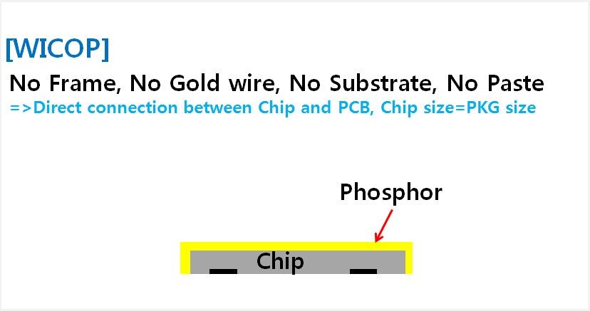
Wicop (Wafer Level Integrated Chip on PCB) is a totally new concept LED product which overcame the limits of the existing CSP (Chip Scale Package). Seoul Semiconductor succeeded in developing and producing the product for the first time in the world in 2012. Because it is designed to directly connect the chip to PCB, there is no need for packaging process such as die bonding or wire bonding. In addition, as there is no intermediate substrate, the size of the chip and package is 100% the same. It is characterized by the super mall size and high efficiency. It is also good for the high luminance and thermal conductivity.
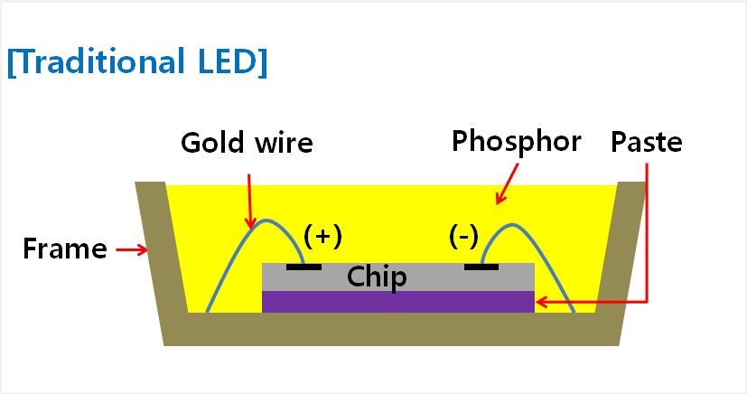
In the case of the currently widely used product of TOP LED, a lot of materials are required for the product such as Die Bonding equipment to attach the chip to the lead frame, Wire Bonding equipment to connect electrodes to the gold wire, and lead frame, gold wire, and adhesives in each process. As the conventional LED needs such packaging process (commonly referred to as die bonding and wire bonding process) and it has a package size larger than the chip size, the size of the chip could not be made smaller.
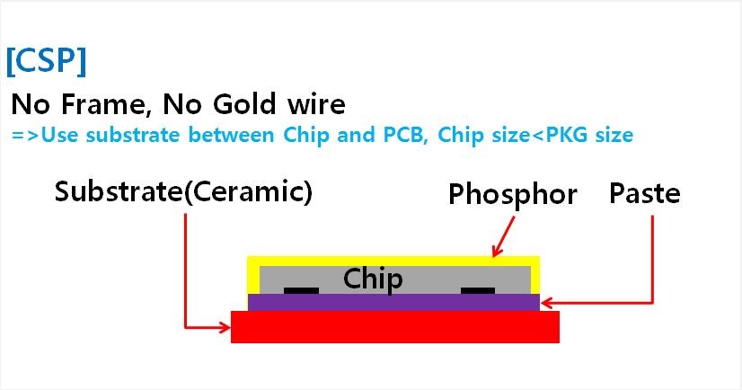
The CSP (Chip Scale Package) technology derived from silicon semiconductors is a technology to miniaturize the size of semiconductor parts (package) to the size of a chip. Generally, when the size of the package does not exceed more than 1.2 times the chip, it is classified as CSP. This technology was applied to the LED industry and companies such as P announced products using this technology in 2012. However, because products using such technology need die bonding equipment, intermediate substrate or ceramic or silicon material to attach the chip to the PCB, it was difficult to see the technology as a complete CSP.
[Comparison of LED production process – General LED, CSP, WICOP]

|
|
General LED Package structure. |
 |
|
CSP: Use of intermediate substrate between Chip and PCB structure. |
 |
|
Wicop: Direct connection between Chip and PCB structure. |
Seoul Semiconductor released for the first time in the world a complete concept of Wicop products in which the size of the package (PKG) is the same with that of chip and does not use other main materials by directly attaching the chip to the PCB. It started to mass produce relevant products and supply them to client companies, thus firmly establishing its position as the leading company in the industry. Also, it secured a global patent regarding Wicop and succeeded in constructing a technological barrier.
Since 2013, Wicop has been supplied to main customers for use as LCD backlight (BLU: Back Light Unit) and camera flash and is also used as head lamps of vehicles. By releasing LED package Wicop2 for use for lamp using Wicop technology this time, Seoul Semiconductor has been able to possess a Wicop product portfolio applicable to all fields of LED industry. Seoul Semiconductor plans to actively target a LED lighting-source market in lights, vehicle, and IT parts currently estimated to be approximately 20trillion ($20B) through the new concept LED Wicop.
Kibum Nam or Head of Central Research Center of Seoul Semiconductor, emphasized that “through the development of Wicop which is an innovative small sized, highly efficient LED technology, the effective value of packaging equipment which was once essential in semiconductor assembly process will noticeably decrease. As all of the parts which had been used for more than 20 years will not be necessary any more, there will be a huge change in the future LED industry” and that “Seoul Semiconductor already has acquired hundreds of global patent portfolio regarding Wicop and takes a close look at how other manufacturers would develop the similar products using the similar technology”.


 CN
TW
EN

