(Author: Judy Lin, Chief Editor, LEDinside)
Grenoble-based research institute CEA LETI (LETI) recently shared with LEDinside how it is transforming nanowire technology first designed for transistors into making ultra-bright LEDs.
There are currently three types of MOSFET designs available on the market, the mainstream Fin Field Effect Transistor (FinFET), a 3D MOSFET technology, Fully Depleted-Silicon on Insulator (FD-SOI) MOSFET and nanowire technology.
“The industry is conservative when it comes to using new (semiconductor) materials, so we still mostly use silicon-based technology,” said LETI’s CEO Marie-Noelle Semeria in an exclusive interview with LEDinside. “You have to justify and convince the industry to use new materials.”
 |
|
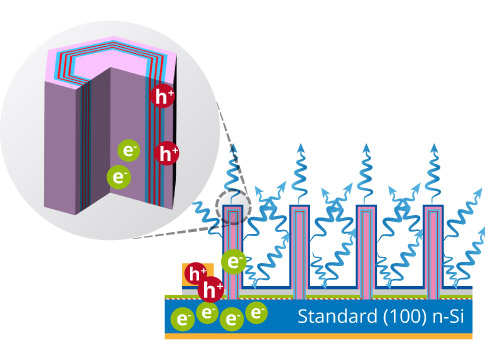
Aledia, a spin-off from LETI's, 3D GaN based nanowire LED technology. (Image courtesy of Aledia) |
Despite the general industry inclination to use more cost effective materials, III-V group semiconductor materials, such as GaN offer better performance in certain driver and optical applications, she explained.
Silicon based nanowires were first developed for transistor applications, but in 5-7 nanometer sized applications LETI is focusing on 3D GaN nanowires for lighting applications.
GaN nanowire 3D LEDs have the advantage of being extremely bright reaching 107 nits, while OLEDs typically only are capable of illuminating 10,000 nits, said Semeria.
LETI’s 3D GaN LEDs are about 10 times brighter than another French based research institute Université Grenoble Alpes, which reported its nanowire LEDs had a brightness of 106 nits.
In LEDs, nanowires can facilitate light extraction because of their wave guiding properties, according to research submitted by a team from France Université Grenoble Alpes to Nano Letters.
Some challenges in working with GaN substrates in nanowires is the epitaxy, the quality of the buffer, ensuring the epitaxies are defect free to optimize light conversion, and patterning of the epitaxy layer. LETI’s diamond display, for instance uses patterned GaN epiwafers instead of a thin epiwafer layer.
However, she was optimistic that GaN LEDs were fully compatible with displays and integration onto silicon wafers.
The GaN LED also needs to be stacked to control each individual nanowire LED to provide good electrostatic control, explained Semeria.
Some other advantages of 3D GaN nanowire LEDs compared to conventional 2D LEDs is less droop, and the capability of placing several different color LEDs onto the same wafer or chip, according to Aledia.
In 2011, LETI carved out this particular research division into start-up company Aledia, which specializes in the manufacturing of 3D GaN nanowire LEDs.
Aledia closed a series B funding worth US $31 million last June, attracting automotive lighting leader Valeo, IKEA GreenTech the venture capital arm of IKEA to invest in its technology.
References


