Micro LED is an enticing display technology considerably future-proof yet hard to fully realize. All already-known challenges are basically induced by three key factors: the size, material, and number of LED chips. The industry refers to a LED chip as a Micro LED chip when its size is below 100μm—almost as tiny as the diameter of human hair. Different colors of Micro LEDs are made with different materials. Some companies attempt to develop a solution for chips of all colors, while the others invent several approaches to transfer, bond, and drive Micro LEDs produced with different compounds. What about the Number of Micro LEDs used for a display, let’s say, a TV, for example? It’s going to be single- to double-digit millions of them.
The manufacture is hard, and so is the testing. To learn more about what could improve in testing processes, LEDinside had an interview with Hidekazu Kotera, Vice Section Manager, and Yoshiyuki Yokoe, Department Manager of Planning & Administration at Toray Engineering, on what progress the company has made in that regard.
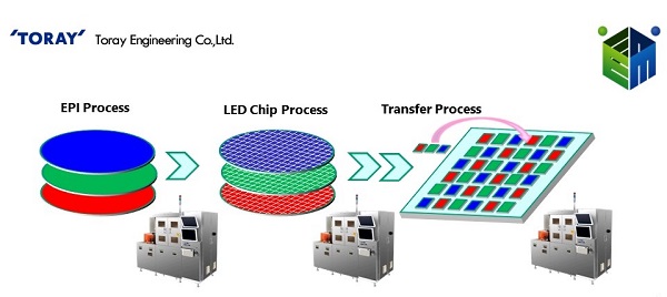
Toray Engineering, a Japan-based production facilities company, has a long history of providing manufacturing and testing equipment specifically for both the semiconductor and display industries. Kotera introduced at 2017 Micro LED International Symposium the company’s semiconductor-level testing equipment, the INSPECTRA series, which is able to test and control the quality of Micro LEDs using photoluminescence (PL) tests.
 |
|
(Image: Toray Engineering) |
Contactless Be the Best for the Tiniest
Photoluminescence (PL) inspection refers to a testing method to assess the status or quality of a substance from its emission of light after absorbing visible or ultraviolet light, also known as fluorescence. The energy of the light source is normally higher than the band gap to trigger the effect. Toray has downsized this technology to be a micro PL (μ PL) measurement, through which optical signals are created and transmitted to the computer that later processes the calculation and forms images based on the firm’s self-developed algorithms, Kotera explained. The inspection is conducted 100% automatically at high speed and intended for both frontend and backend wafer processing.
PL imaging is not a new approach as it is long used for testing other applications such as PV cells, whereas it could be innovative when it comes to inspection of optical devices such as LED, compared to electroluminescence (EL) testing. EL testing, on the other hand, inspects defects by giving an electric current that passes through devices to see if they emit light or not. It often proceeds with a probe contact.
However, incumbent probes- even if some of them are with the smallest lateral size of 125μm- are not small enough to test parameters of Micro LED. The contact-based test might even damage the chips. “Testing with light enables simple and quick inspection of several million chips on a wafer and the advantage makes our machine an effective alternative to the probe inspection,” said Kotera.
Multi-stage Quality Control via Inspect-and-Trims
The INSPECTRA series can be used at multiple stages in the manufacture of Micro LED along with the LMT series, Toray’s laser micro trimming system, said both Kotera and Yokoe. The former tests the components while the latter trims off defective parts, enabling inspect-and-trim processes at multiple stages to control the quality of Micro LED.
Knowing the stringent standards for Micro LED wafer production, Toray makes its equipment available at the early stage of the production to inspect the deposition quality after epitaxial growth. The thickness of the epitaxial layer has to be in the range between 3-5μm and the wavelength uniformity has to be high enough (±0.5nm), according to LEDinside analysts. The machine is able to show if inspected wafers meet the requirements with images such as wafer/substrate maps. It then trims off non-uniform parts accordingly.
Kotera explained that the equipment can also be used before and after the mass transfer of Micro LED. It particularly solves incurred post-transfer problems including external defects, dislocation of the chips, and bonding failure. The inspection machine would send data and signals to the laser trimming tool when detecting failures to remove damaged parts or parts that are not successfully transferred or placed while keeping the rest area intact.
Very few AOI machine manufacturers with know-hows of PL inspection are able to provide solutions to inspect the quality of a Micro LED display module after the mass transfer, which makes Toray stand out, stressed Kotera.
Yokoe said the company plays a crucial part in improving the yield and managing the quality of Micro LED technology with its edges. Its proprietary technologies keep the level of production quality high, reduces the cost of repair, raises the yield rate, and eventually speeds up the manufacturing processes.
LEDinside got exclusive data from Toray that it has currently offered over 400 units of the INSPECTRA series to companies both inside Japan and abroad in countries including Taiwan and China. 80% of the distribution was in Japan, while 20% was overseas. However, it is unknown whether companies purchasing the equipment use it for the production of Micro LED. Toray expected more demand to come in the next few years considering the urge of developers to mass produce Micro LED and the incremental anticipation in the market.
The managers kept their lips tight when asked if the company by any chance considers developing its own mass transfer technology as effective as its inspection methods. Yet, they said they would continue their development and provide better solutions with more desired technology to customers in the advanced technology industry.
( Hidekazu Kotera and Yoshiyuki Yokoe from Toray Engineering were interviewed by Roger Chu, Joanne Wu, and Evangeline Huang. The article was written by Evangeline Huang, Editor, LEDinside.)


