Display Week, held in every May in Los Angles, is the world-famous Display Exhibition. As the raising attention toward Micro LED market, LEDinside will provide the latest display market news LIVE.

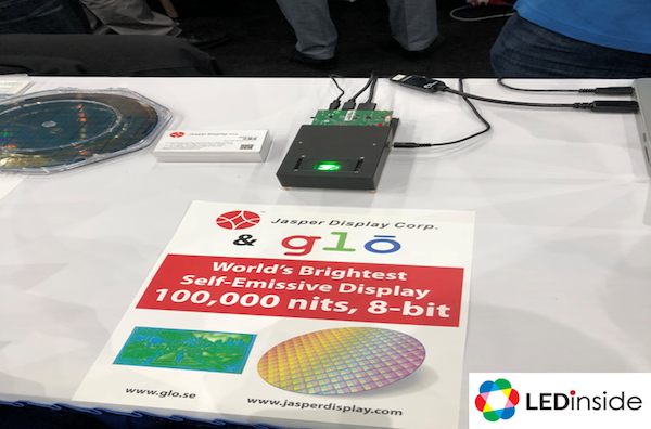
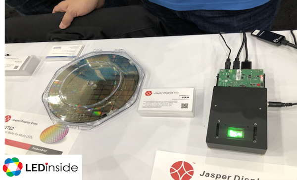
At Display week 2018, glō and Jasper Display Corp. (JDC) will, for the first time ever, demo the world's brightest self-emitting display panel. The industry's brightest μLEDs (10 μm), developed and integrated by glō, paired with JDC's new silicon backplane, the JD67E2, make it possible to deliver the high brightness and contrast that will benefit the next wave of watches, phones, heads-up-displays (HUDs), and augmented reality (AR) products.
The demonstration is around 0.7-inch single-color display with revolution 640x350 and 230 thousand micro-LED, which can reach to 100 ppi. LED lights up based on green monochrome panel and can reach 8-bits greyscale.
With the JD67E2 the μLED industry can take advantage of silicon that is tailored for the needs of high performance μLED devices. JDC’s expertise in digitally modulated pixel arrays is the key to their lead in μLED-focused silicon platforms. JDC’s history of developing industry firsts has made it possible to anticipate the rise of μ LEDs. Jeffrey Li, Director of Applications, is excited about the new product possibilities that JDC's new silicon opens up for customers worldwide.

“Our JD67E2 silicon backplane demonstrates our ability to deliver on the promise of μLEDs. We’re excited to offer what the industry has been waiting for - silicon that has been designed to realize super- bright μLED panels. glō's super-high efficiency μLEDs, coupled with their silicon integration expertise, made it possible to demo a blindingly bright self-emissive display - the brightest in the world. Our μLED backplane technology can be customized on a per-project basis, allowing us to make specialized silicon suiting needs ranging from low-power AR headsets all the way to projection displays.”
The full-color capable JD67E2 die features a resolution of 1920 x 1080, a pixel pitch of 8 um, and offers excellent current uniformity via a proprietary current source pixel. Uniformity is better than 1% across the array. The device-ready die is now shipping as part of the JD27E2 8" wafer product. JDC’s DFM methodologies enable high-yield volume production of their wafers.
Author: Roger / LEDinside


